Search for answers or browse our Knowledge Base.
Guides | Models | Validation | Book
Rectangular Microstrip Patch Antennas: A Comparative Analysis of Transmission Line Theory and AN-SOF Numerical Results
This comprehensive study explores the design and electromagnetic behavior of the rectangular microstrip patch antenna, contrasting classical transmission line theory with AN-SOF numerical simulations. By evaluating resonance, input impedance, and the impact of finite vs. infinite substrates, the article details the specific areas where analytical formulas align with full-wave results and where complex phenomena like surface waves and mutual conductance necessitate advanced computational validation.
The Transition from 3D Structures to Planar Integration
Classical wire antenna structures such as dipoles, monopoles, loops, helices, and complex dipole arrays have long served as the backbone of radio frequency communication. However, these traditional designs are inherently three-dimensional and bulky, presenting significant mechanical challenges when integration with modern, high-density planar electronics is required. As electronic devices have shrunk in size while increasing in complexity, the need for a radiator that shares the same physical form factor as the integrated circuits (ICs) and transmission lines powering them became paramount. The microstrip patch antenna emerged as the definitive solution to these constraints, offering a seamless bridge between electromagnetic radiation and planar circuitry.
The conceptual origins of the microstrip radiator date back to the early 1950s, with G. Deschamps providing foundational contributions in 1953. Despite this early groundwork, it was not until the 1970s that the technology gained widespread momentum and commercial viability. This maturation was catalyzed by the work of Robert “Bob” Munson in 1972, whose innovations transformed the patch antenna from a laboratory concept into a practical engineering tool. The surge in popularity during this era was closely tied to the advancement of stable dielectric materials and the development of sophisticated manufacturing techniques, allowing the microstrip patch to evolve into a standard component for aerospace and terrestrial applications.
Physical Characteristics and Modern Applications
The microstrip patch antenna is defined by its low-profile geometry, lightweight construction, and extreme cost-effectiveness. Because it can be fabricated using standard printed circuit board (PCB) photolithography, it allows for high-precision manufacturing at a very low per-unit cost. These antennas are often conformable, meaning they can be mounted on curved surfaces, such as the fuselage of an aircraft or the body of a missile, without significantly altering the vehicle’s aerodynamic profile. These features make the technology indispensable for modern consumer and specialized electronics, including mobile smartphones, GPS receivers, Wi-Fi routers, and satellite communication links where space and weight are critical design variables.
Physical Structure of the Rectangular Patch Antenna
In its most fundamental form, a microstrip patch antenna is a multi-layered structure consisting of a radiating metallic “patch” situated on one side of a thin dielectric substrate. The opposite side of this substrate is covered by a continuous metallic ground plane, which serves as both a return path for current and a shield to minimize back-radiation.
The radiating patch is the primary component responsible for the antenna’s performance. While a diverse variety of geometries, including circular, triangular, and elliptical shapes, have been explored, the rectangular patch remains widely utilized. Its prevalence is due to its relative ease of analysis, predictable polarization characteristics, and straightforward design procedures (Fig. 1). The dielectric substrate plays a dual role: it provides mechanical support for the patch and helps determine the electrical size of the antenna through its relative permittivity, allowing the physical dimensions to be reduced compared to antennas operating in free space.
To achieve optimal performance, a microstrip feed network is carefully designed to excite the patch. This network is engineered to ensure precise impedance matching, which is critical for minimizing return losses and suppressing cross-polarization levels that could otherwise degrade signal integrity.
When these antennas are installed on complex platforms such as aircraft, ships, or terrestrial vehicles, the conductive ground plane plays a fundamental role. It acts as an electromagnetic reflector, directing the radiated energy into the upper hemisphere. This creates a directional radiation pattern characterized by moderate gain and a relatively wide bandwidth. These attributes make rectangular microstrip antennas particularly effective for satellite links and high-speed mobile communication systems where a focused beam is required to maintain reliable connectivity.
The physical architecture of a rectangular microstrip patch antenna is defined by the arrangement depicted in Fig. 2. Each component must be dimensioned to satisfy the resonance requirements of the desired operating frequency.
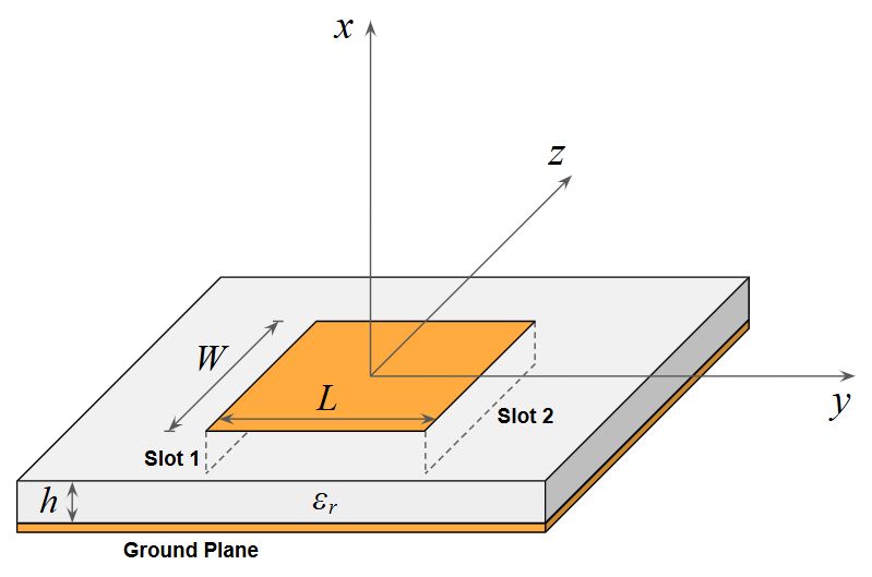
1. The Ground Plane
The base of the antenna consists of a continuous conductive sheet that covers the entire lower surface of the dielectric substrate. This plane serves a dual purpose: it acts as a return path for the high-frequency currents and ensures that the antenna radiates predominantly in one direction. By acting as a shield, it also prevents the antenna’s near-fields from interfering with the electronic components located beneath the mounting surface.
2. The Dielectric Substrate
The substrate is a thin dielectric layer characterized by its height $h$ and its relative permittivity $\varepsilon_{r}$. The height of the substrate is a critical parameter in determining the antenna’s efficiency and bandwidth. In standard designs, the substrate thickness is kept significantly smaller than the free-space wavelength to ensure proper operation:
$\displaystyle h \ll \lambda_{0} $
Typically, the height is selected within the following range:
$\displaystyle 0.005 \lambda_{0} \le h \le 0.05 \lambda_{0} $
A thicker substrate generally leads to increased bandwidth and improved radiation power, but it also risks the excitation of surface waves. These surface waves can travel along the lateral direction, leading to energy loss and distortions in the radiation pattern.
3. The Radiating Patch
The top layer is the radiating patch, a rectangular metallic conductor defined by its length $L$ and width $W$. For the purpose of mathematical modeling and simulation, the patch is usually assumed to be very thin, allowing its physical thickness to be neglected without compromising the accuracy of the results. The length $L$ is the most influential dimension, as it is approximately a half-wavelength within the dielectric medium, directly determining the antenna’s resonance at the operating frequency.
Methods of Antenna Excitation
The method used to deliver energy to the patch is chosen based on the application’s mechanical requirements and the desired electrical characteristics.
- Coaxial Probe Feed: In this method, a coaxial cable is attached to the bottom of the antenna. The outer conductor is connected to the ground plane, while the inner conductor passes through the substrate to make contact with the radiating patch. This technique is highly versatile because the probe can be positioned at any point on the patch, allowing for easy impedance matching by finding the “sweet spot” where the input resistance is 50 Ohms.
- Microstrip Transmission Line: This approach involves a narrow conducting strip printed on the same substrate as the patch. The line is connected directly to the edge of the rectangle. Because the entire antenna and feed can be etched in a single process, this method is very cost-effective. Designers often use an “inset” feed, where the line extends into a notch in the patch, to match the high impedance at the edge of the patch to the characteristic impedance of the transmission line.
- Advanced Coupling Techniques: Beyond direct contact, designers may use proximity coupling or aperture coupling. These non-contact methods use electromagnetic induction to transfer energy between a feed line on a separate layer and the radiating patch. These methods are prized for their ability to provide even wider bandwidths and to reduce the spurious radiation that can sometimes leak from direct-contact feed lines.
Theoretical Framework: The Transmission Line Model
The transmission line model provides the most intuitive and computationally efficient description of the rectangular patch antenna’s resonant behavior. In this framework, the patch is represented by two radiating slots separated by a transmission line of length $L$ (Fig. 2). These slots are located at the opposite edges of the rectangular conductor and are electromagnetically coupled through the fields established within the dielectric substrate. This model effectively treats the patch as a transmission line where the dominant mode of propagation is TEM.
Determination of the Patch Width
The width of the patch, $W$, plays a significant role in determining the radiation resistance and the bandwidth of the antenna. To ensure high radiation efficiency, the width is calculated based on the target resonant frequency and the dielectric properties of the substrate. The width of a resonant rectangular microstrip patch can be calculated as:
$\displaystyle W \,=\, \frac{c}{2f_r} \, \sqrt{\frac{2}{\varepsilon_r \,+\, 1}} \qquad (1)$
where $f_{r}$ is the desired resonant frequency and $c$ is the speed of light in free space.
The Effective Dielectric Constant
Because the patch is situated on a substrate of finite thickness, the electromagnetic fields are not contained entirely within the dielectric material. Instead, a portion of the field lines extends into the air region surrounding the antenna, a phenomenon known as fringing. To account for this non-homogeneous environment, an effective dielectric constant, $\varepsilon_{\text{eff}}$, is introduced. This parameter provides an equivalent uniform medium that represents the combined electromagnetic effect of the substrate and the surrounding air. The effective dielectric constant is given by:
$\displaystyle \varepsilon_{\text{eff}} \,=\, \frac{\varepsilon_r \,+\, 1}{2} \,+\, \frac{\varepsilon_r \,-\, 1}{2} \left( 1 \,+\, 12 \, \frac{h}{W} \right)^{-1/2} \qquad (2)$
Resonant Length and the Fringing Effect
For a microstrip antenna to radiate efficiently, it must operate at resonance, which occurs when the electrical length of the patch is approximately one-half of a wavelength within the dielectric medium. The physical length $L$ required to achieve this half-wavelength resonance is naturally shorter than that of an ideal half-wave dipole in free space. The effective length required for resonance is calculated as:
$\displaystyle L_{\text{eff}} \,=\, \frac{c}{2 f_r \sqrt{\varepsilon_{\text{eff}}}} \qquad (3)$
However, the physical dimensions of the patch must be further refined due to the fringing effect. Because the electromagnetic fields extend beyond the physical edges of the metallic patch, the antenna appears electrically longer than its actual measured dimensions.
To account for this behavior, an additional length increment, $\Delta L$, is introduced to represent the extension of the field at each edge of the patch. Consequently, the actual physical length $L$ of the patch is determined by subtracting these extensions from the effective length:
$\displaystyle L \,=\, L_{\text{eff}} \,-\, 2\Delta L \,=\, \frac{c}{2 f_r \sqrt{\varepsilon_{\text{eff}}}} \,-\, 2\Delta L \qquad (4)$
An online calculator implementing the above formulas and in depth explanations of rectangular patch antenna can be found here:
The Coaxial Probe Feeding Method
The coaxial probe feed is one of the most versatile and widely implemented techniques for exciting a microstrip patch antenna. In this configuration, a coaxial connector is attached to the back of the ground plane. The outer conductor of the cable is bonded to the ground plane, while the inner conductor extends through a small hole drilled in the dielectric substrate to make direct contact with the radiating patch at a specifically chosen coordinate $(y_0, z_0) $ (Fig. 3).
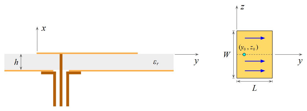
This method is highly prized for its mechanical robustness and its ability to facilitate precise impedance matching. Because the input resistance of the patch varies significantly across its surface, the designer can “tune” the antenna to a standard 50-Ohm system simply by adjusting the physical location of the probe. The most common configuration involves placing the feed point at the midpoint of the patch width $W$, specifically along the longitudinal centerline where $\displaystyle z_0 = 0$ (Fig. 3).
Resonant Input Resistance
The resonant input resistance $R_{\text{in}}$ at the probe location varies according to the square of the modal field distribution within the cavity formed by the patch and the ground plane. As the probe moves from the center of the patch toward the radiating edge, the resistance increases following a cosine-squared relationship:
$\displaystyle R_{\text{in}} \,=\, R_e \, \cos^2\left(\frac{\pi \, y_0}{L}\right) \qquad (5)$
In this equation, $R_e$ represents the resonant resistance measured exactly at the radiating edge of the patch. At the center of the patch ($y_0 = L/2$), the input resistance is at its minimum, while it reaches its maximum value at the edges ($y_0 = 0$).
The resistance at the radiating edge, $R_e$, is linked to the radiation properties of the two slots that represent the patch in the transmission line model (Fig. 2). It is given by:
$\displaystyle R_e \,=\, \frac{1}{2G} \qquad (6)$
where $G$ is the radiation conductance of a single radiating slot. The factor of two in the denominator accounts for the presence of the two slots acting in parallel. For patches where the substrate thickness $h$ is small compared to the wavelength, the radiation conductance can be approximated as:
$\displaystyle G \,=\, \frac{W}{120\,\lambda_0} \left(1 \,-\, \frac{(k_0 \,h)^2}{24}\right) \quad \text{for} \;\; h < 0.1\lambda_0 \qquad (7)$
where $\lambda_0$ is the free-space wavelength and $k_0 = 2\pi/\lambda_0$ is the free-space wavenumber.
Implementing the Rectangular Patch Model in AN-SOF
To validate the theoretical framework established by the transmission line model, we present a numerical model of a rectangular microstrip patch antenna developed using the AN-SOF simulation suite. The antenna is designed to resonate at $f_r = 2.4 \text{ GHz}$, a frequency central to the Industrial, Scientific, and Medical (ISM) band used in Wi-Fi and Bluetooth applications. The design utilizes a dielectric substrate with a relative permittivity of $\varepsilon_r = 4.4 $ and a height of $h = 1.6 \text{ mm}$, parameters that correspond to standard FR4 epoxy glass material.
Geometric Specification and Meshing Strategy
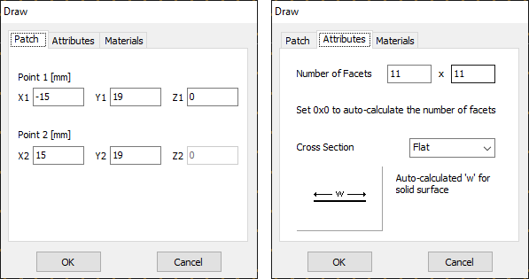
Based on the analytical formulas previously presented, the initial physical dimensions for the resonant patch were determined to be $W = 38 \text{ mm}$ and $L = 30 \text{ mm}$ (rounded to two significant digits). Within the AN-SOF environment, the rectangular patch is generated by defining the spatial coordinates of two opposite corners along its diagonal.
Given that the resonant dimensions are approximately one-half wavelength within the dielectric medium, the surface was discretized into a mesh of $11 \times 11$ facets. This level of refinement provides a balanced trade-off between computational speed and the accuracy of the induced surface current density. Figure 4 illustrates the specific coordinate definitions within the Patch window and the corresponding facet specifications used to build the antenna geometry.
The dielectric substrate is set in the Setup > Environment panel, where the Substrate configuration parameters are assigned (Fig. 5).
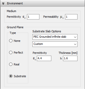
A fundamental assumption in the classical transmission line model is that both the dielectric substrate and the conductive ground plane are infinite in their lateral extent. This simplification allows for the isolated study of the patch’s radiating slots without the influence of edge and corner diffraction from a finite board. To maintain consistency with the theoretical predictions, the AN-SOF model initially utilizes the “PEC Grounded infinite slab” option. This ensures that the numerical results can be compared directly to the analytical formulas without introducing variables related to the physical size of the PCB.
Simulation Results and Validation
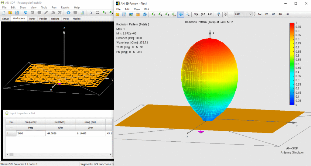
Figure 6 displays the rectangular patch antenna within the AN-SOF workspace, superimposed with the normalized radiation pattern in a linear scale. The pattern is directional, exhibiting a well-defined main lobe with a beamwidth of about $80^\circ$ and no appreciable secondary lobes, as expected for this configuration.

The quantitative validation is found in the input impedance results. At the target frequency of $2400 \text{ MHz}$, the input impedance table reports a value of approximately:
$\displaystyle Z_{\text{in}} \,=\, 45 \,+\, j 6 \, \Omega$
This result indicates that the antenna is nearly at resonance, as the reactive component of the impedance is small. Furthermore, the real part of the impedance ($45 \, \Omega$) is remarkably close to the standard $50\,\Omega$ characteristic impedance used in RF transmission lines. This proximity suggests a high-quality impedance match with a low Voltage Standing Wave Ratio ($\text{VSWR} \approx 1.2$), validating that the analytical dimensions provided an accurate starting point for the numerical design.
Numerical Modeling of the Coaxial Feed and Impedance Alignment
In the AN-SOF environment, the physical coaxial probe is modeled by inserting a vertical wire between the radiating patch and the ground plane. This wire is assigned a radius of 0.5 mm to approximate the dimensions of a standard SMA connector inner conductor and is positioned at a distance of 8.2 mm from the center of the patch, which serves as the coordinate origin. A voltage source is applied to this vertical segment to simulate the excitation.
Calculating the exact feed position is an important step in achieving a 50-Ohm match. For this specific model, the feed point is located at a distance of $L/2 \,-\, 8.2 \text{ mm} = 6.8 \text{ mm}$ when measured from the radiating edge. It is important to note that this value differs from the theoretical $9.6 \text{ mm}$ predicted by the cosine-squared approximation in formula (5). Such discrepancies between analytical models and full-wave numerical simulations are expected. Theoretical formulas for resonant input resistance are based on several simplifications, most notably the neglect of mutual conductance between the two radiating slots and the exclusion of the probe’s own parasitic inductance. Numerical solvers like AN-SOF provide a more rigorous account of these near-field interactions, leading to a more accurate determination of the optimal feed placement.
Directivity, Gain, and the Impact of Surface Waves
The simulation provides detailed insights into the energy distribution of the antenna. AN-SOF reports a directivity of $7.9 \text{ dBi}$ but a significantly lower gain of approximately $2 \text{ dBi}$. This disparity is due to a calculated radiation efficiency of $26\%$. In electromagnetics, the dimensionless directivity $D$ and gain $G$ are fundamentally linked by the radiation efficiency $\eta$ through the relation:
$\displaystyle G \,=\, \eta D $
Even though the model assumes a lossless dielectric substrate and PEC (Perfect Electric Conductor) surfaces, a large portion of the input power is not radiated into the far-field. In a model utilizing an infinite dielectric substrate, electromagnetic energy excites surface wave modes that propagate laterally within the dielectric layer. Because the substrate is modeled as infinite, this power continues to travel away from the patch indefinitely without ever contributing to the “free space” radiation pattern, resulting in a lower reported efficiency.
These surface-wave losses become more pronounced as the substrate thickness increases or as the relative permittivity rises. In contrast, in a finite-substrate model, these surface waves eventually reach the edges of the board, where they are either reflected or diffracted into space. Consequently, in the finite-substrate example discussed later, the radiation efficiency reaches 100% because ohmic and dielectric losses remain excluded, and all power eventually leaves the structure.
Resonant Behavior and VSWR Characterization
The frequency response of the rectangular patch is best understood through its input impedance and VSWR profiles (Fig. 7). The antenna exhibits the characteristics of a parallel resonance. At the resonant frequency, the input resistance reaches its maximum value while the input reactance undergoes a transition from inductive (positive) to capacitive (negative). This negative reactance slope is a hallmark of parallel resonant systems. Because of this behavior, the rectangular patch antenna can be modeled as a parallel RLC equivalent circuit in the vicinity of the resonance frequency.
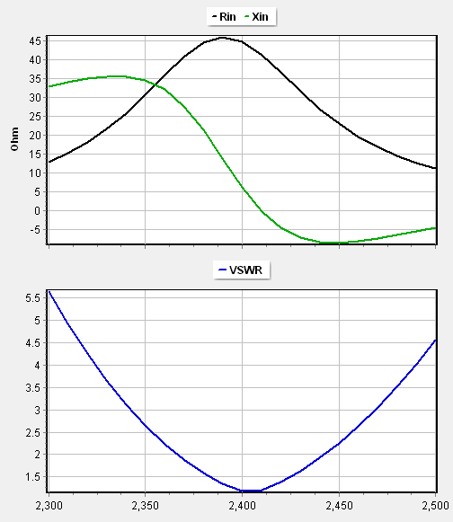
The VSWR curve provides a clear indication of the antenna’s impedance bandwidth. The simulation indicates a bandwidth of approximately 50 MHz for a VSWR threshold of 1.5. This result aligns well with practical engineering expectations for a standard patch on an FR4 substrate, where typical bandwidths range between 20 and 60 MHz. This level of agreement validates the mesh density and the environment settings used in the AN-SOF model.
Comparative Analysis: Infinite vs. Finite Substrates
To provide a more realistic assessment of the antenna’s performance on a physical circuit board, a second model was developed utilizing a finite dielectric slab measuring $100 \text{ mm} \times 100 \text{ mm}$. The impact of the finite boundary is most visible in the radiation pattern comparisons (Fig. 8). When the substrate is infinite, the ground plane acts as a perfect shield, and all radiation is confined to the upper hemisphere.
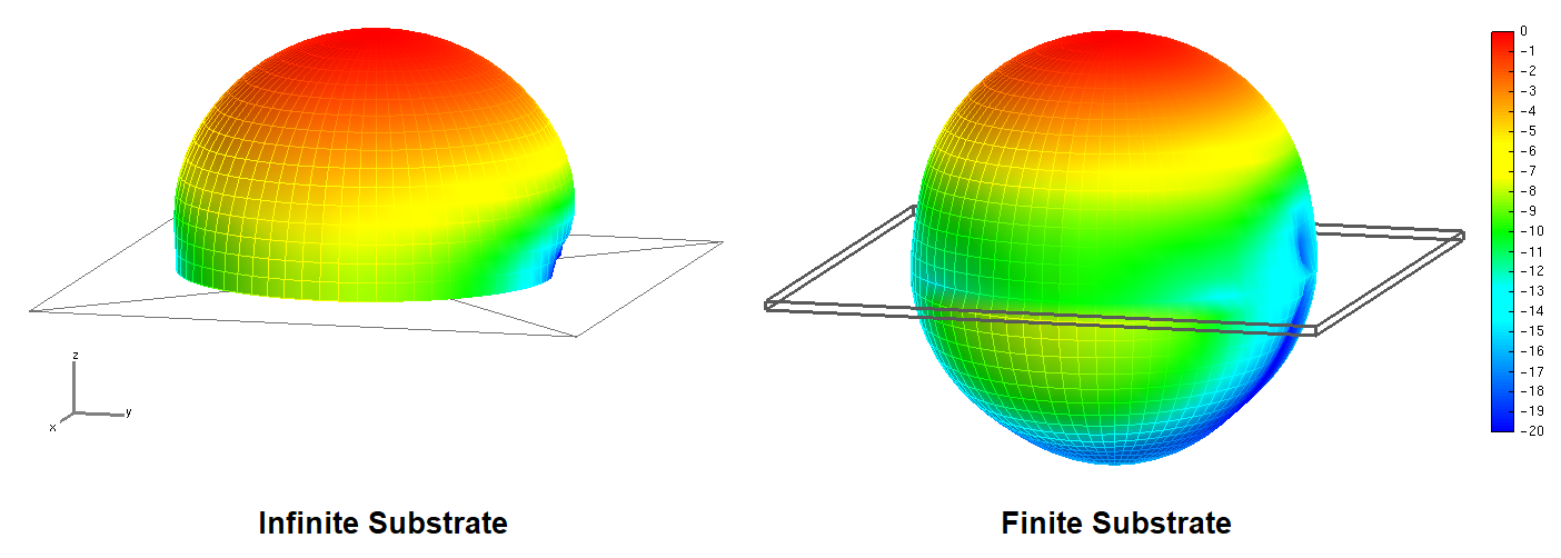
However, with a finite substrate, electromagnetic fields can wrap around the edges of the PCB through edge and corner diffraction. This leads to back-radiation, effectively reducing the main lobe directivity to approximately $2.3 \text{ dBi}$. Despite this significant change in the far-field pattern, the input impedance remains remarkably stable, calculated at $44 + j5 \, \Omega$ at $2.4 \text{ GHz}$. This stability suggests that the infinite substrate model serves as an excellent and computationally efficient first approximation for impedance tuning and feed-point placement. For the final stages of design, however, including the finite dimensions of the substrate is essential for accurately predicting the gain, front-to-back ratio, and potential interference with other nearby components.
Conclusions
This article provides a rigorous assessment of the rectangular microstrip patch antenna, comparing the traditional transmission line model with AN-SOF numerical results at 2.4 GHz. Several key conclusions regarding the design and validation process are established.
Theory as a First-Order Approximation
Transmission line formulas are effective for determining initial dimensions but function only as first-order approximations. They neglect critical higher-order effects, such as the mutual conductance between radiating slots and the parasitic inductance of the coaxial probe. AN-SOF provides the nuanced calculation of input impedance required for precise feed-point refinement. Achieving a stable 50-Ohm match often necessitates sub-millimeter adjustments that analytical theory alone cannot guarantee.
The Impact of Substrate Boundaries
Substrate modeling is decisive in predicting radiation patterns and efficiency. While infinite dielectric models simplify initial impedance tuning, they fail to capture the physical reality of edge diffraction and back-radiation. Finite substrate simulations provide a comprehensive view of far-field performance, accounting for the wrapping of fields around the PCB boundaries.
Furthermore, the simulation identifies how surface wave treatment affects reported efficiency. In infinite models, power coupled into surface waves is treated as “lost” as it propagates laterally to infinity, potentially underestimating radiation efficiency. In contrast, the finite model correctly demonstrates that this energy eventually reaches the board edges, where it radiates or diffracts.
In summary, full-wave numerical analysis is an essential final step. It allows the designer to account for complex near-field interactions and environmental diffraction, ensuring that idealized formulas translate into reliable real-world antenna performance.
See Also:
Technical Keywords: Microstrip Patch Antenna, Transmission Line Model, Resonant Frequency, Fringing Effects, Effective Dielectric Constant, Coaxial Probe Feed, Input Impedance Matching, Radiation Efficiency, Surface Waves, Infinite vs. Finite Substrates.