AN-SOF Antenna Simulation Software
Accurate, Fast, and Easy-to-Use Tool for Antenna Modeling, Analysis, and Design
Welcome to AN-SOF!
Congratulations on choosing AN-SOF, the best combination of ease of use and accuracy you can find in an electromagnetic simulator for the modeling and design of antennas and wire structures in general. This User Guide describes AN-SOF and its many features in detail. Here, you will also find step-by-step examples and tips to help you quickly progress with your antenna modeling projects.
Table of Contents
📖 Getting Started
⚙ Simulation Setup
✏ Drawing Wires
📡 Grids and Surfaces
🔌 Sources and Loads
📶 Incident Field
🛣 Ground Planes
🧮 Running Calculations
📈 Displaying Results
➡ Transmission Lines
📗 Step By Step
🎓 Background Theory
❓ Frequently Asked Questions
Join a Global Community of RF Experts
Our technical insights are trusted by engineers and antenna enthusiasts at top-tier firms and research institutions. See how they use AN-SOF →
Getting Started
Enhancing Antenna Design Through Simulation Software
An antenna model represents a real-world antenna within a computer program. It is important not to confuse this type of model with a scale model, which is sometimes constructed to measure the radiation characteristics of a larger, physically identical antenna. Due to the mathematical complexity involved in modeling, specialized software is often used to predict and analyze antenna performance.
Computer simulation plays a critical role in overcoming challenges and driving innovation throughout the product development lifecycle. A computer model offers significant advantages, including the ability to modify, redesign, break, destroy, and rebuild designs multiple times without wasting physical materials. By leveraging simulation software, engineers and antenna designers can significantly reduce the costs associated with building successive physical prototypes, streamlining the design process.
AN-SOF is a comprehensive simulation software suite designed for antenna modeling and optimization. It supports the design of a wide range of wire antennas, including dipoles, monopoles, Yagis, log-periodic arrays, helices, spirals, loops, horns, fractals, phased arrays, and many other types. Additionally, AN-SOF enables detailed modeling of feeding systems using transmission lines, allowing users to analyze complex antenna configurations with precision. The software can simulate antennas positioned above lossy ground planes or broadcast antennas above radial wire ground screens, providing realistic and accurate results.
Furthermore, AN-SOF’s calculation capabilities have been extended to include single-layer microstrip patch antennas and the computation of radiated emissions from Printed Circuit Boards (PCBs). As a result, AN-SOF is a powerful tool for Electromagnetic Compatibility (EMC) applications. The software also supports passive circuits with lumped impedances and non-radiating networks, enabling comprehensive analysis of antenna systems.
📝 Note
In the realm of antenna applications, AN-SOF proves invaluable as it empowers users to achieve the following:
- Design superior antennas.
- Predict and optimize antenna performance.
- Fine-tune antenna parameters for optimal results.
- Account for environmental effects on antenna performance.
- Employ script-based optimization to refine designs.
- Gain valuable insights into antenna behavior.
- Experiment multiple times prior to physically building the antenna model.
- Deepen understanding of antennas and their properties.
- Facilitate knowledge sharing and collaboration with colleagues.
With AN-SOF at your disposal, you can explore the exciting possibilities of antenna analysis and optimization. The software provides an extensive toolkit for designing, evaluating, and enhancing antenna performance, empowering engineers and enthusiasts alike to push the boundaries of innovation.
📝 Note
AN-SOF enables us to perform a wide range of tasks, including:
- Describing the antenna’s geometry accurately.
- Selecting appropriate construction materials.
- Specifying the environmental and ground conditions.
- Determining the antenna’s height above the ground.
- Analyzing the radiation pattern and front-to-back ratio.
- Plotting directivity and gain.
- Evaluating impedance and SWR (Standing Wave Ratio).
- Predicting bandwidth.
- Obtaining numerous additional parameters and plots.
Drawing the geometry of structures in AN-SOF is intuitive and user-friendly. Wires can be created in a 3D space using the mouse, menus, and easy-to-navigate dialog windows. Tools are available to zoom, move, and rotate the structure, ensuring precise control over the design process.
To visualize simulation results, AN-SOF integrates seamlessly with a suite of specialized applications: AN-XY Chart, AN-Smith, AN-Polar, and AN-3D Pattern. These tools allow users to display graphs and analyze data effectively. They can also be executed independently for further graphic processing, offering flexibility and convenience for advanced users.
With AN-SOF and its software suite for displaying graphics, we have all the necessary tools to guide us through the stages of an antenna design process.
Introduction to AN-SOF: Antenna Simulation Essentials
AN-SOF performs computations of electric currents flowing on metallic structures, including antennas in transmitting and receiving modes, as well as scatterers. A scatterer refers to any object capable of reflecting and/or diffracting radiofrequency waves. For instance, wave scattering analysis can be conducted on the surface of an aircraft to determine optimal antenna placement, on a parabolic reflector to examine gain in relation to the reflector shape, or on a car’s chassis to predict interference effects.
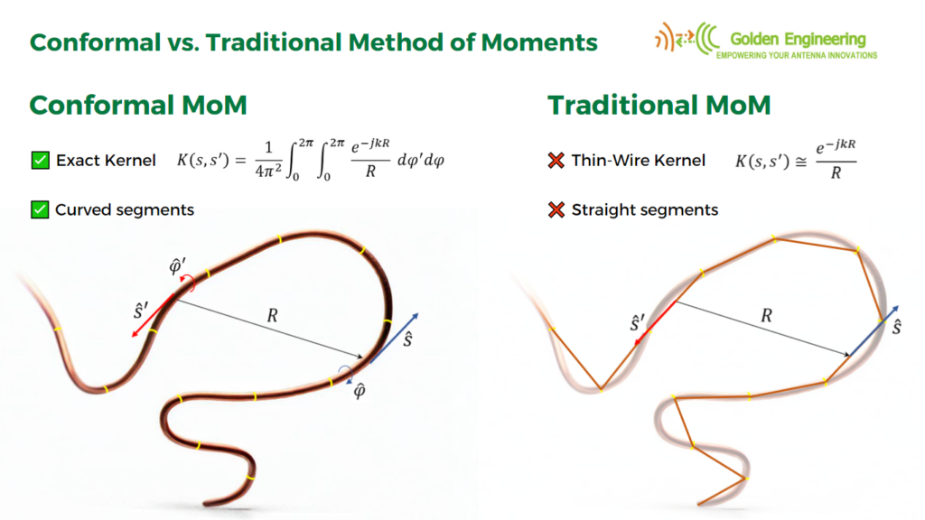
The Method of Moments (MoM) stands as one of the most widely validated techniques for antenna simulation. AN-SOF incorporates an enhanced and advanced version of this method called the Conformal Method of Moments (CMoM) with Exact Kernel, which addresses various challenges associated with traditional MoM approaches and achieves unparalleled accuracy.
Interested in learning more about the CMoM implementation in AN-SOF? Read this article:
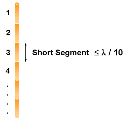
According to the MoM, any metallic structure can be represented using conductive wires, as illustrated in Fig. 1. These wires are subdivided into small segments, which assume the shape of cylindrical tubes. To obtain accurate results, the length of each wire segment should be comparatively short compared to the wavelength, as depicted in Fig. 2. However, this concern can be alleviated during the initial simulation since AN-SOF automatically handles the segmentation of wires.
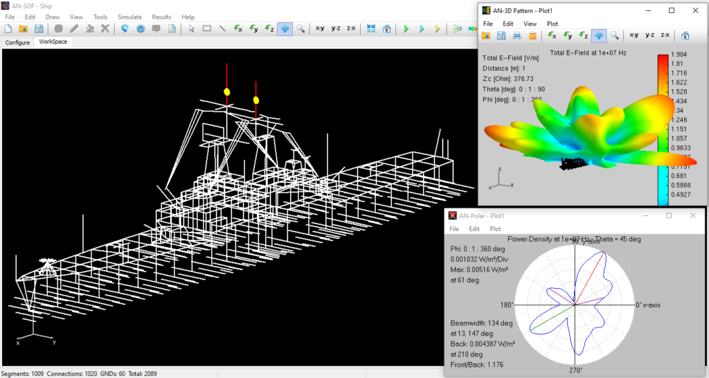
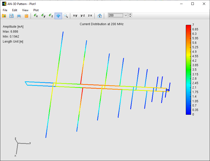
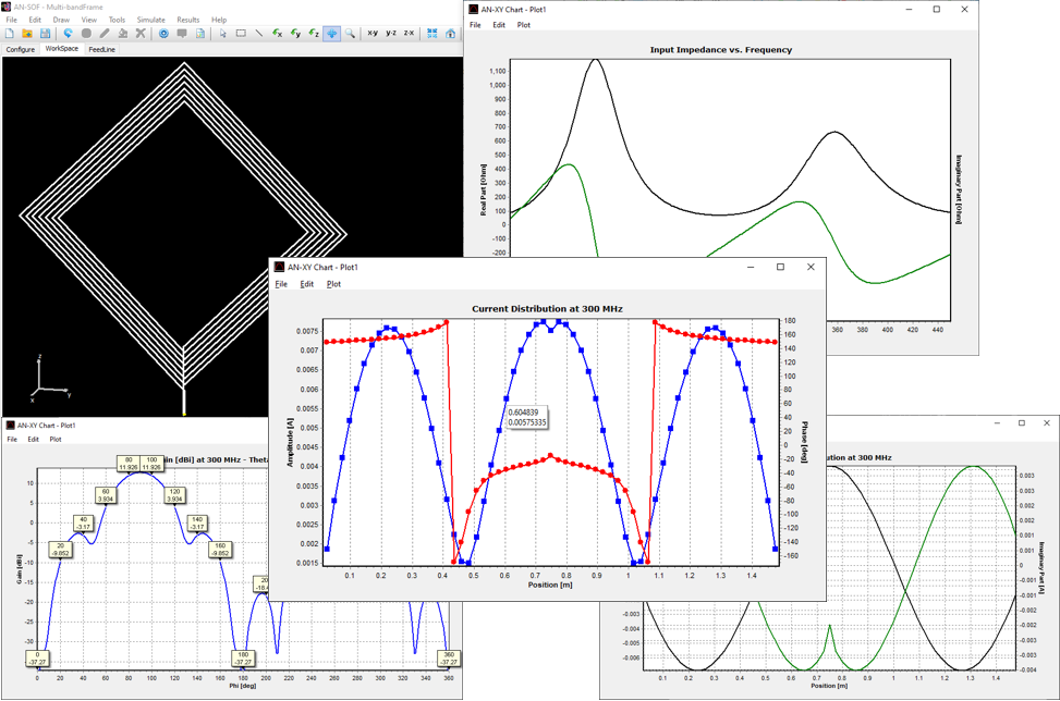
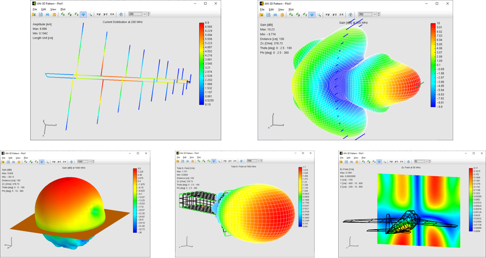
The flow of electric currents within the structure can be achieved by introducing a voltage generator at a specific location operating at a given frequency. Current generators can also serve as the excitation source, alongside plane waves impinging on the structure from distant sources. Once the geometry, materials, and sources of the structure are defined, the computation can be executed to determine the currents flowing through the wire segments. Generally, these electric currents exhibit varying intensities along and across the structure, collectively referred to as a current distribution. Fig. 3 showcases an example of the current distribution on a log-periodic antenna.
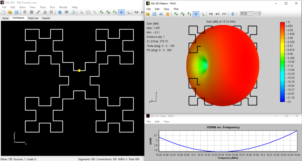
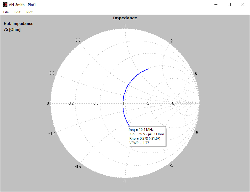
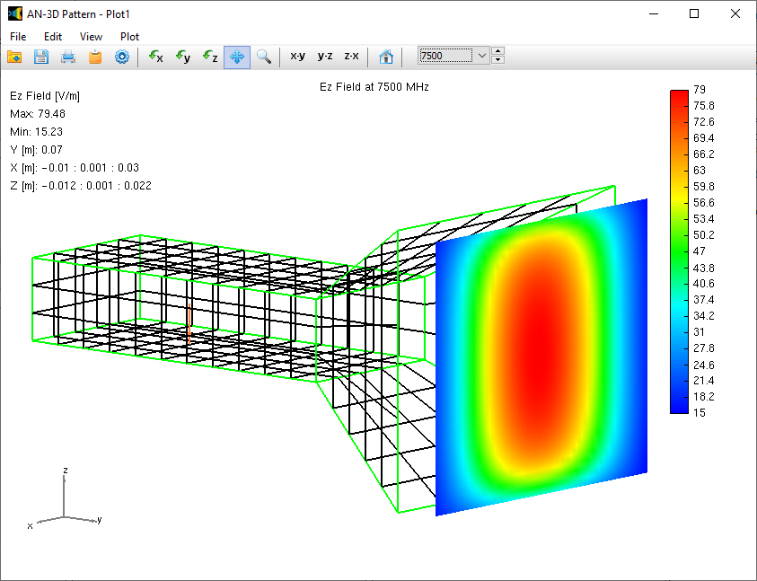
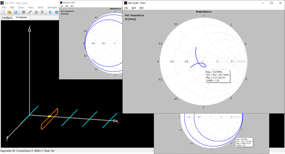
In the subsequent phase of the simulation process, the electromagnetic field radiated by the current distribution can be calculated. However, the current distribution itself provides valuable insights into the behavior of the structure, particularly when a frequency sweep is conducted. In the case of antennas, the feed point impedance can be analyzed as a function of frequency to assess the bandwidth. The Voltage Standing Wave Ratio (VSWR) can be plotted on a Smith chart for better interpretation of the results, as demonstrated in Fig. 4. The electric and magnetic fields in the proximity of the structure, known as the near-field zone, can be obtained and visualized as a color map, with intensities often resembling temperature maps used in weather forecasts, as shown in Fig. 5.
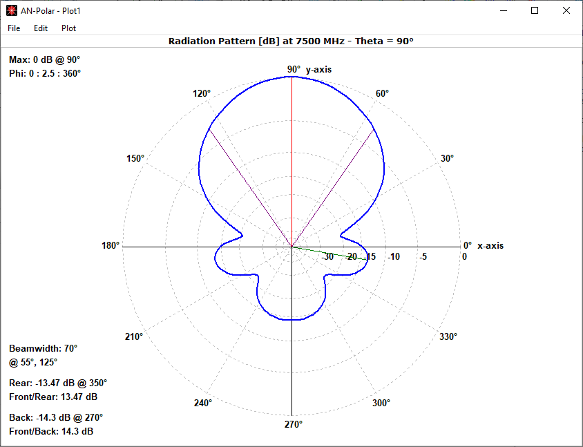
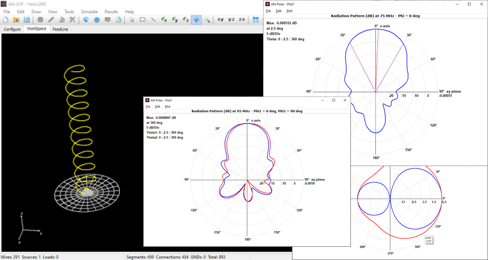
In the far-field zone, situated several wavelengths away from the structure, the magnetic field becomes proportional to the electric field. As a result, the electric field intensities are commonly used to analyze the results. This region is depicted in polar diagrams, as illustrated in Fig. 6, where the radiated field is represented as a function of direction. A more comprehensive representation can be achieved by plotting a 3D pattern, where radiation lobes can be superimposed onto the structure’s geometry, providing enhanced visualization of its directional properties, as exemplified in Fig. 7.
Explore Our Pre-Computed Examples in the Models Tab
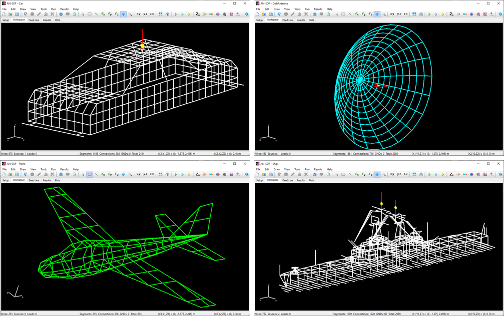
AN-SOF includes a collection of pre-calculated models that enable users to quickly load example projects directly into the interface. These models are organized into categories for easy navigation, making this feature especially useful for users exploring example designs and learning key antenna concepts.
In the Models tab, you’ll find quick-access buttons for opening example models (see Fig. 8). Each model displays a 3D radiation pattern and includes a PDF guide with informational resources. Since all models are pre-calculated, they can be opened and explored using the AN-SOF Trial version.
The total number of segments used in each model is displayed after the “|” symbol on each button label in the Models tab, as well as in the Status Bar at the bottom of the AN-SOF window. This total includes:
- Wire segments
- Wire-to-wire junctions
- Wire-to-ground connections (labeled as “GNDs”)
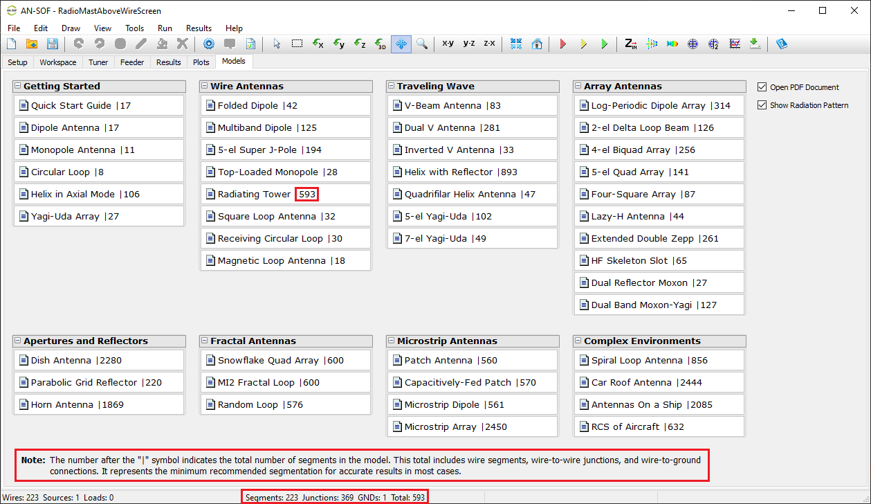
Note:
The AN-SOF Trial version supports models with up to 50 total segments. If you modify an example model and exceed this limit, you’ll need an active license for the AN-SOF PRO Edition to run additional simulations.
To explore the example models, simply click the buttons in the Models tab. On the right side of the screen, you can use the options “Open PDF Document” and “Show Radiation Pattern” to toggle the display of the PDF guide or the radiation pattern plot as needed.
AN-SOF delivers an unmatched combination of peak simulation accuracy and an intuitive, streamlined user interface. Ready to experience the power of the Conformal Method of Moments firsthand? Let’s execute your first simulation.
Join a Global Community of RF Experts
Our technical insights are trusted by engineers and antenna enthusiasts at top-tier firms and research institutions. See how they use AN-SOF →
Performing the First Simulation with AN-SOF
As a first experience using AN-SOF, let’s simulate a standard half-wave dipole, which is one of the simplest antennas that can be modeled. A dipole is a straight wire that is fed at its center. When the wire’s cross-section is circular, it is referred to as a cylindrical antenna. Since the wire is typically made of a highly conductive material, it can be considered a perfect conductor with zero resistivity. Therefore, we will model a cylindrical antenna with zero resistivity in this example. Follow the steps below to perform this simulation.
Step 1: Setup
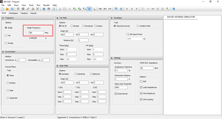
The first step is to set the operating frequency. Navigate to the Setup tab in the AN-SOF main window. Within the Frequency panel, there are three options to choose from. Select Single and enter the operating frequency for the antenna (see Fig. 9). In this case, the frequency is given in megahertz (MHz), and lengths are measured in meters (m). If desired, you can change the unit system for frequencies and lengths by going to Tools > Preferences. Please note that for a frequency of 300 MHz, the wavelength is approximately 1 meter (0.999308 m).
Step 2: Draw
Once the operating frequency has been set, you can draw the antenna geometry on the Workspace tab. The workspace is where the wire structure is visualized, representing a 3D space that allows zooming, rotation, and movement.
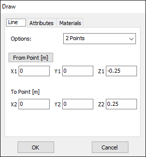
In AN-SOF, a straight wire is referred to as a Line. To draw a line, go to the main menu and select Draw > Line. This will open the Draw dialog box. In the Line tab, you can set the coordinates of two distinct points.
For this example, we will create a line along the z-axis that is 0.5 meters long, corresponding to half a wavelength at 300 MHz. Figure 10 illustrates the chosen starting point of the line at (X1, Y1, Z1) = (0, 0, -0.25) m, and the ending point at (X2, Y2, Z2) = (0, 0, 0.25) m. Next, switch to the Attributes tab (see Fig. 11). To ensure accurate results, the line should be divided into segments that are relatively short compared to the wavelength. Generally, a segment length equal to or less than one-tenth of a wavelength is considered short. AN-SOF suggests a minimum number of segments to achieve reliable results automatically. If you require higher resolution, you can increase the number of segments.
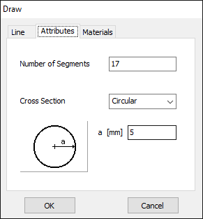
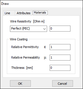
In this case, the line will be divided into 17 segments, and the wire cross-section will be circular with a radius of 5 millimeters. On the Materials tab (refer to Fig. 12), you can set the wire’s resistivity to zero.
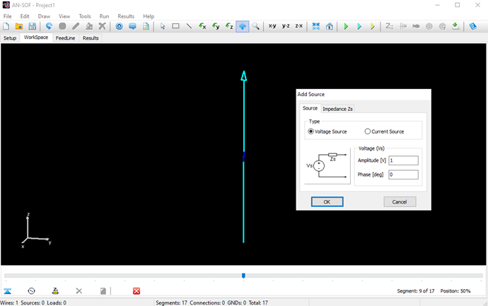
The next step is to feed the dipole. Right-click on the wire and select the Source/Load/TL command from the pop-up menu that appears. A toolbar with a slider will be displayed at the bottom of the screen. Move the slider to the segment located at the center of the wire. Then, click the Add Source button. Add a voltage source with an amplitude of 1 Volt and a phase of zero (see Fig. 13).
Step 3: Run
To run the calculation, go to Run > Currents Only (Ctrl + R) in the main menu. Once the calculations are completed, proceed to Run > Far-Field in the main menu. This will calculate the current distribution on the dipole antenna and the radiated field.
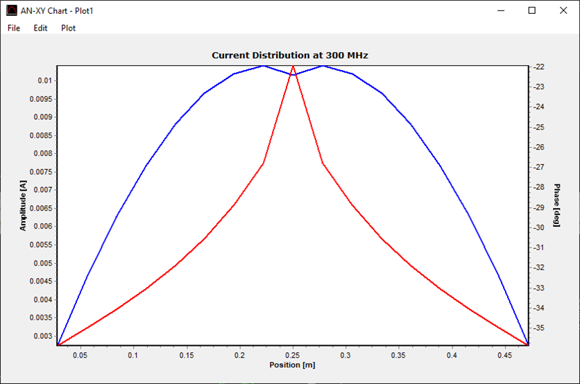
AN-SOF provides integrated graphical tools for result visualization. Right-click on the wire and select Current Profile 2D from the displayed pop-up menu. A plot showing the current distribution in amplitude along the dipole antenna will be displayed (refer to Fig. 14). Since a half-wave dipole has been drawn, the resulting current distribution resembles a semi-cycle approaching a sine function.
You can obtain several parameters from the perspective of the voltage source connected to the antenna terminals. Right-click on the wire and select Current vs. Freq. from the pop-up menu. Move the slider to the position of the voltage source and click on the Input List button. This will display the input impedance of the dipole antenna, along with many other parameters (see Fig. 15).
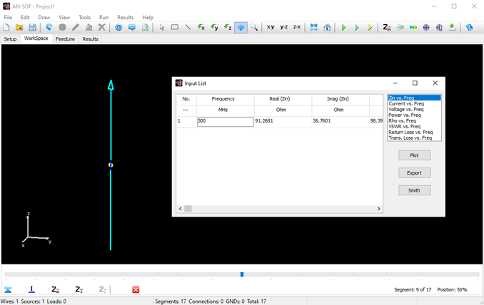
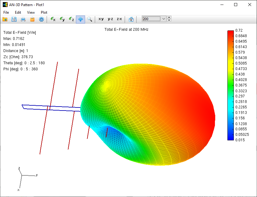
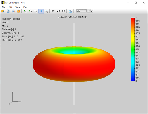
Alternatively, you can obtain the input impedance by simply clicking on the Input Impedance Table (ZIN) button in the main toolbar. To represent the radiation pattern in a 3D plot, navigate to Results > Far-Field Angular Plot > 3D Radiation Pattern in the main menu. The normalized radiation pattern will be displayed in the AN-3D Pattern application. A color bar-scale indicates the field intensities over the radiation lobes. Additionally, you can plot the directivity, gain, and electric field patterns by accessing the Plot menu in AN-3D Pattern. In the case of a half-wave dipole, it exhibits omnidirectional characteristics in the plane perpendicular to the dipole axis (xy-plane) (see Fig. 16).
As you have just experienced, a simulation consists of three simple steps. We hope you have enjoyed this example. For additional step-by-step examples, please visit our section titled Examples > Step by Step.
Summary
The key advantages of AN-SOF can be summarized as follows:
- AN-SOF is antenna modeling and design software that offers fast and user-friendly input and output graphical interfaces.
- AN-SOF employs the Conformal Method of Moments with Exact Kernel, resulting in enhanced accuracy and speed.
- AN-SOF provides an extended frequency range, enabling simulations from extremely low frequencies (such as 60 Hz circuits) to microwave antennas.
Simulating a wire structure involves a three-step procedure:
- Setup: Set frequencies, environment, and desired results.
- Draw: Draw the geometry, specify materials, and add sources.
- Run: Perform the calculation and visualize the results.
At the beginning of the simulation, you can choose a convenient unit system for frequencies and lengths. This choice can be adjusted later by accessing Tools > Preferences. For instance, wire lengths are typically measured in meters (m) or feet (ft) for frequencies below 100 MHz, while millimeters (mm) or inches (in) are commonly used for higher frequencies.
Features and Capabilities
AN-SOF is a comprehensive software tool for the modeling and simulation of antenna systems and radiating structures in general.
AN-SOF is intended for solving problems in the following areas:
- Modeling and design of wire antennas.
- Antennas above a lossy ground plane.
- Broadcast antennas over radial wire ground screens.
- Single layer microstrip patch antennas.
- Radiated emissions from printed circuit boards (PCBs).
- Electromagnetic Compatibility (EMC) applications.
- Passive circuits, transmission lines, and non-radiating networks.
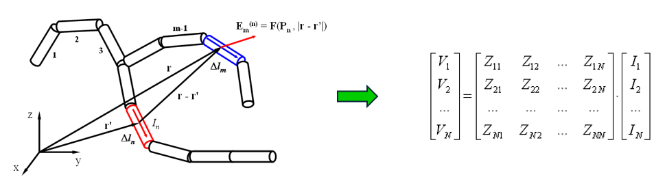
AN-SOF is based on an improved version of the so-called Method of Moments (MoM) for wire structures. Metallic objects like antennas can be modeled by a set of conductive wires and wire grids, as it is illustrated in Fig. 1. In the MoM formulation, the wires composing the structure are divided into segments that must be short compared to the wavelength. If a source is placed at a given location on the structure, an electric current will be forced to flow on the segments. The induced current on each individual segment is the first quantity calculated by AN-SOF.
Once the current distribution has been obtained, the radiated electromagnetic field can be computed in the far- and near-field zones. Input parameters at the position of the source or generator can also be obtained, such as the input impedance, input power, standing wave ratio (SWR), reflection coefficient, transmission loss, etc.
The modeling of the structure can be performed by means of the AN-SOF specific 3D CAD interface. Electromagnetic fields, currents, voltages, input impedances, consumed and radiated powers, directivity, gain and many more parameters can be computed in a frequency sweep and plotted in 2D and 3D graphical representations.
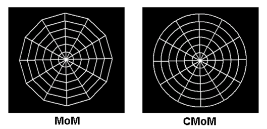
In the case of curved antennas like loops, helices, and spirals, the MoM in AN-SOF has been improved to accurately account for the wire’s exact curvature. Traditional calculations often use straight-line segments to approximate curved antennas, resulting in many discontinuous wire junctions. This linear approximation can be inefficient in terms of computer memory and the number of calculations required, as it necessitates multiple straight segments to mimic the smooth curvature of wires. To address this issue, AN-SOF uses curved segments that precisely follow the contours of curved antennas. This innovative technique is known as the Conformal Method of Moments (CMoM).
As an example, Fig. 2 shows the different approaches to a circular disc obtained by means of the MoM and CMoM methods. Both methods are available in AN-SOF since the MoM is a special case of the more general CMoM.
In addition to the CMoM capabilities, advanced mathematical techniques have been implemented in the calculation engine making possible simulations from extremely low frequencies (e.g., electric circuits at 50-60 Hz) to very high ones (e.g., microwave antennas above 1 GHz).
In what follows, a summary of the modeling options and the simulation results that can be obtained from AN-SOF is presented.
Modeling of Metallic Structures
Metallic structures can be modeled by combining different types of wires, grids, and surfaces:
Wires
Wire Grids and Solid Surfaces
- All types of curved wires can be modeled by means of arced or quadratic segments.
- Wire grids and solid surfaces can be defined using either curved or straight wire segments. Curved segments follow the exact curvature of discs, rings, cones, cylinders, spheres, and parabolic surfaces. Grids are composed of cylindrical wires that leave holes between them, while solid surfaces are composed of flat wires or strips that cover the surface without leaving holes between them.
- Tapered wires with stepped radii can be defined.
- All wires can be loaded or excited at any segment.
- The structure can also have finite non-zero resistivities (skin effect).
- Electrical connections of different wires and connections of several wires at one point are possible.
- Metallic wires in either dielectric or magnetic media can be analyzed.
- Wires with insulation can be modeled. Dielectric and magnetic coatings are available.
- The structures can be placed in free space, over a perfectly conducting ground plane or over an imperfect ground plane.
- Flat strip lines can be defined on a dielectric substrate for modeling planar antennas and printed circuit boards (PCB).
- Vias in microstrip antennas and printed circuit boards can also be modeled.
- The wire cross-section can either be Circular, Square, Flat, Elliptical, Rectangular or Triangular.
- Transmission lines can be connected to the metal structure. There are over 160 cable models available, including two-wire and coaxial cables, with characteristic impedance, velocity factor, and loss parameters adjusted to actual datasheets.
- The geometry modeling can be performed in suitable unit systems (um, cm, mm, m, in, ft). Different unit systems can also be chosen for inductance (pH, nH, uH, mH, H) and capacitance (pF, nF, uF, mF, F).
Excitation Methods
- Voltage sources can be placed on the wires, as many as there are segments, with equal or different amplitudes (RMS values) and phases.
- Current sources (e.g., representing impressed currents) can also be arranged at any segments.
- The voltage and current sources can have internal impedances.
- An incident plane wave of arbitrary polarization (linear, circular, or elliptical) and direction of incidence can also be used as the excitation.
- Hertzian electric and magnetic dipoles can also be modeled and used as the excitation.
- The antenna input power can be set to obtain the results (current distribution, near and far fields) scaled accordingly.
Frequency options
- The simulation can either be performed for a single frequency, for frequencies taken from a list or for a frequency sweep.
- The list of frequencies can either be created inside the program or loaded from a text file. It can also be saved to a txt file.
- Linear and logarithmic frequency sweeps are possible.
- A suitable unit system can be selected (Hz, KHz, MHz, GHz).
Data Input
- 3D CAD tools are implemented for drawing and modifying the structure geometry, including wires, grids, surfaces, discrete generators, and lumped loads.
- The segmentation of wire geometry can be done automatically or manually.
- Left-clicking on a wire selects and highlights it. Right-clicking on a wire reveals a pop-up menu with various options.
- Wire connections are easily established by copying and pasting the endpoints of wires.
- Special 3D symbols indicate the positions of sources, load elements, and ground points.
- All dialog boxes validate inputs for accuracy.
- The program includes mouse-supported functions for rotating, moving, and zooming.
- Transmission lines can be easily entered into a table, which serves as a library, for later use. A line is highlighted in the graphical interface for easy identification.
- The program allows you to import geometrical data from text files. It supports three different file formats for importing wires, including the NEC (Numerical Electromagnetics Code) cards. Additionally, it can import DXF files containing 3D LINE entities.
- The AN-SOF architecture integrates powerful numerical methods to achieve the fastest calculation speed and the most accurate results.
Data Output
- All computed data is stored in files for subsequent graphical analysis.
- Input impedances, currents, voltages, VSWR, S11, return and transmission losses, radiated and consumed powers, efficiency, directivity, gain, and other system responses are presented as lists in text format and can be plotted against frequency. A Smith chart is available to represent impedances and admittances, as well as to display the reflection coefficient and VSWR at the selected point on the graph.
- The current distribution on a selected wire can be plotted in amplitude, phase, real, and imaginary parts against position in a 2D representation. The currents flowing on a structure can also be plotted as a color map on the wires.
- Radiation and scattering fields are obtained, including power density, directivity and gain patterns, total electric field, linearly and circularly polarized components, axial ratio, and Radar Cross Section (RCS). The surface-wave field can be determined as a function of distance in the case of a real ground with finite conductivity.
- Near-field components can be calculated in Cartesian, cylindrical, and spherical coordinates. Field intensities can be plotted in 2D and 3D graphical representations and visualized as color maps in the proximity of a structure.
- A 2D representation of radiated fields is available in Cartesian and polar coordinates. The ARRL-style log scale can be applied to polar diagrams.
- 3D radiation patterns can be viewed from arbitrary angles with zoom functions, colored mesh and surface representations, and a color bar scale. 3D patterns can be plotted with specially designed lighting and illumination for enhanced visualization of simulation results.
- Far-field patterns can be separated into theta (vertical) and phi (horizontal) linearly polarized components, as well as right and left circularly polarized components. The axial ratio and the front-to-rear and front-to-back ratios are shown in polar plots and can be displayed as a function of frequency.
- The frequency spectrum of near- and far-fields can be visualized in a 2D representation for all field components across different frequencies.
- An average radiated power test, also known as AGT (Average Gain Test), is conducted to verify the accuracy of the simulation.
- The calculated data can be exported to .csv, .dat, or .txt files for use in other software programs.
- An embedded transmission line calculator is included to simplify the design of feed lines for transmitting antennas. Actual cable part numbers can be selected from a wide range of manufacturers, thanks to data extracted from cable datasheets and integrated into the calculator.
- A Bulk Simulation feature enables the automated calculation of multiple files, each with different geometric descriptions, to obtain results based on variable geometric parameters. The results are automatically exported to .csv files for further processing.
- You can choose suitable unit systems for the plotted results, including current scaling (KA, A, mA, uA), voltage scaling (KV, V, mV, uV), electric field scaling (KV/m, V/m, mV/m, uV/m), magnetic field scaling (KA/m, A/m, mA/m, uA/m), decibel scales, and more.
Integrated graphical tools
AN-SOF has a suite of integrated graphical tools for the convenient visualization of the simulation results. The following applications are installed automatically and used by the main program, AN-SOF:
AN-XY Chart app
A friendly 2D chart for plotting two related quantities, Y versus X. Use AN-XY Chart to plot parameters that depend on frequency, such as currents, voltages, impedances, reflection coefficient, VSWR, S11, radiated power, consumed power, directivity, gain, radiation efficiency, radar cross section, field components, axial ratio, and many more. Also plot the current distribution along wires as a function of position, 2D slices of radiation lobes and near fields as a function of distance from an antenna. Choose different units to display results and use the mouse to easily zoom and scroll graphs.

AN-Smith app
Plot impedance or admittance curves on the Smith chart with this tool. Just click on the graph to get the frequency, impedance, reflection coefficient, VSWR, and S11 that correspond to each point on the curve. Plots can be stored in independent files and opened later for a graphical analysis with AN-Smith.

AN-Polar app
Plot on a polar diagram the radiation pattern versus the azimuth (horizontal) or zenith (vertical) angles. The maximum, -3dB and minimum radiation levels are shown within the chart as well as the beamwidth and front-to-rear/back ratio. Click on the graph to quickly obtain the values of the radiated field. The represented quantities include power density, directivity, gain, normalized radiation pattern, total electric field, linearly and circularly polarized components, axial ratio, and radar cross section (RCS).

AN-3D Pattern app
Get a complete view of the radiation properties of a structure by plotting a 3D radiation pattern. AN-3D Pattern implements colored mesh and surface for the clear visualization of radiation lobes, including a color bar-scale indicating the field intensities over the lobes. Quickly rotate, move, and zoom the graph using the mouse. The 3D radiation pattern can be superimposed to the structure geometry to gain more insight into the directional properties of antennas.
The represented quantities include the power density, normalized radiation pattern, directivity, gain, total field, linearly and circularly polarized components, axial ratio, and Radar Cross Section (RCS). Choose between linear or decibel scales. Display near fields as color maps in the proximity of antennas in three different representations: Cartesian, cylindrical and spherical plots. Also plot the current distribution on the structure as a colored intensity map.
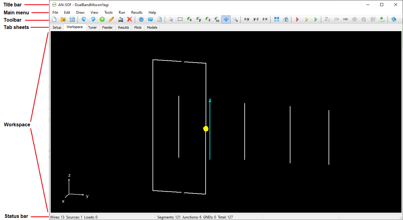
Main Window and Menu
When AN-SOF starts, the main window displays several key components that form the core of the user interface (Fig. 1):
- Title Bar – Displays the name of the currently active project file (
.emmformat). - Main Menu Bar – Provides access to the primary menus: File, Edit, Draw, View, Tools, Run, Results, and Help.
- Toolbar – Contains icons for quick access to commonly used commands and tools.
- Tab Sheets – Allow users to switch between different stages of the workflow, from Setup to Plots, with a single click.
- Workspace – The central 3D canvas where wire structures are drawn and visualized.
- Status Bar – Displays real-time information, such as the number of segments, wire-to-wire junctions, and wire-to-ground connections (GNDs).
File Menu
The File menu provides commands for managing AN-SOF projects, including creating, opening, saving, importing, and exporting files. The available commands are:
- New… (Ctrl + N)
Creates a new project from scratch. - Open… (Ctrl + O)
Opens an existing project file (.emm) using the standard Open dialog. - Save (Ctrl + S)
Saves the current project under its existing name. - Save As…
Saves the current project with a new name. If the project is new, this command prompts the user to assign a name and location. - Import Wires
Opens a dialog to import wire data from various formats, including AN-SOF (.wre), NEC (.nec), and MM format (.txt). - Export Wires
Allows exporting the wire geometry to several formats:- NEC (
*.nec) - DXF (
*.dxf) - Scilab script (
*.sce) - MATLAB/Octave script (
*.m)
- NEC (
- Copy Workspace
Copies the current workspace view to the clipboard as a bitmap image. - Recent Files List
Displays up to ten recently opened project files for quick access. Use “Empty Recent Files List” to clear the history. - Exit (Ctrl + Q)
Closes the current project and exits AN-SOF.
Edit Menu
The Edit menu provides tools for modifying, organizing, and managing wires in your project. The available commands include:
- Undo (Ctrl + Z)
Reverts the project to the previous state before the last command was executed. - Redo (Ctrl + Y)
Reapplies the last undone action, restoring the project to the state before Undo was used. - Source / Load / TL (Ctrl + Ins)
Opens the Source/Load/TL toolbar, allowing you to add sources, loads, or connect transmission line (TL) ports to a selected wire segment. This command is enabled when a single wire is selected. - Modify (Ctrl + M)
Opens the Modify dialog box for editing properties of the selected wire(s). Available when one or more wires are selected. - Wire Color
Opens a standard color selection dialog to change the color of the selected wire(s). Enabled when one or more wires are selected. - Delete (Ctrl + Del)
Deletes the selected wire(s), including any attached sources or loads. Enabled when one or more wires are selected. - Copy Start Point
Copies the start point coordinates of the selected wire. This point can be used as the start of a new wire, enabling direct connection. Enabled when a wire is selected. - Copy End Point
Copies the end point coordinates of the selected wire for use as the starting point of a new, connected wire. Enabled when a wire is selected. - Start Point to GND
Draws a vertical wire from the start point of the selected wire down to the ground plane. This command is available only when a ground plane is defined in the model and a wire is selected. - End Point to GND
Draws a vertical wire from the end point of the selected wire down to the ground plane. Like the previous command, it is available when a ground plane exists and a wire is selected. - Move Wires… (Ctrl + Alt + M)
Opens the Move Wires dialog to reposition the selected wires. Enabled when at least one wire is selected. - Rotate Wires… (Ctrl + Alt + R)
Opens the Rotate Wires dialog to rotate selected wires around a specified axis. Enabled when at least one wire is selected. - Scale Wires… (Ctrl + Alt + S)
Opens the Scale Wires dialog to apply a scaling factor to the selected wires. Enabled when at least one wire is selected. - Copy Wires…
Opens the Copy Wires dialog to duplicate the selected wires, with options to apply translation or rotation to the copies. Enabled when at least one wire is selected. - Stack Wires…
Opens the Stack Wires dialog to generate multiple copies of the selected wires arranged along a specified direction. Enabled when at least one wire is selected.
Draw Menu
The Draw menu provides tools for creating a wide variety of wire geometries and wire grids. These commands allow users to model antenna elements with precision and flexibility. The available options include:
- Line
Opens the Line dialog box to draw a straight wire between two defined endpoints. - Arc
Opens the Arc dialog to draw a circular arc segment. - Circle
Opens the Circle dialog to draw a complete circular loop. - Helix
Opens the Helix dialog to create a helical wire, often used in axial-mode antennas. - Quadratic
Opens the Quadratic dialog to draw a curved wire defined by a quadratic function. - Archimedean Spiral
Opens the Archimedean Spiral dialog to draw a spiral with uniform spacing between turns. - Logarithmic Spiral
Opens the Logarithmic Spiral dialog to create a spiral with exponentially increasing spacing—ideal for frequency-independent antenna designs.
Wire Grid / Solid Surface
This option creates a wire grid or a discretized surface geometry. It includes the following sub-commands:
- Patch – Draws a rectangular mesh on the xy-plane.
- Plate – Creates a bilinear surface or flat panel.
- Disc – Draws a flat circular disc.
- Flat Ring – Draws a ring-shaped disc with a central hole.
- Cone – Creates a conical surface structure.
- Truncated Cone – Draws a cone with a flat top (cut-off cone).
- Cylinder – Draws a cylindrical surface.
- Sphere – Creates a spherical grid or surface.
- Paraboloid – Draws a parabolic reflector surface.
Tapered Wire
This option allows drawing wires with stepped-radius profiles, useful for simulating tapered elements such as monopoles or matching sections. Each command mirrors the standard wire options above (e.g., Line, Arc, Helix), but with the ability to assign different radii along the length.
- Tabular Input (Ctrl + T)
Opens a spreadsheet-style table for entering linear wires, sources, loads, and transmission lines numerically—ideal for precise control and batch input. - Transmission Lines (Ctrl + L)
Opens a dedicated table to define transmission lines by specifying their characteristic impedance, velocity factor, length, and loss parameters.
View Menu
The View menu provides options to control the display of interface elements, adjust zoom levels, and access additional project and wire information. Use these commands to customize your workspace and enhance your modeling experience:
- Wire Properties… (Ctrl + W)
Opens the Wire Properties dialog, showing detailed information about the selected wire. This command is available when a wire is selected. - Project Details…
Opens the Project Details dialog, displaying a summary of the current project, including the number of segments, wires, sources, and loads. - Zoom In (Ctrl + I)
Magnifies the view within the workspace. You can also zoom in by scrolling the mouse wheel backward. - Zoom Out (Ctrl + K)
Reduces the view scale in the workspace. You can also zoom out by scrolling the mouse wheel forward. - Reset Zoom Scale
Resets the zoom level and resizes the workspace to fit the entire structure. - Axes… (Ctrl + A)
Opens the Axes dialog to adjust the appearance of the coordinate axes. Press F7 to toggle between the small axes (shown in the lower-left corner) and the main axes (centered in the workspace). - X-Y Plane / Y-Z Plane / Z-X Plane
Switches the view to align the selected plane (XY, YZ, or ZX) parallel to the screen, offering easier modeling and inspection from different perspectives. - Center
Centers the view on the structure in the workspace without altering the zoom level. - Initial View (Home)
Resets the workspace to the default orientation and zoom level. - Drawing Panel
Displays a panel on the left side of the workspace with quick-access buttons for drawing wires, wire grids/solid surfaces, and tapered wires.
Tools Menu
The Tools menu provides access to plotting tools, wire checking utilities, and other helpful features for project analysis and customization. The commands available in this menu include:
- 3D Chart
Launches the AN-3D Pattern application to open and view 3D radiation pattern files (.p3d). - Polar Chart
Launches the AN-Polar application for displaying polar radiation patterns from.plrfiles. - Rectangular Chart
Launches the AN-XY Chart application to view rectangular (Cartesian) plots from.pltfiles. - Smith Chart
Launches the AN-Smith application to display impedance or reflection coefficient data from.sthfiles using a Smith chart. - Check Individual Wires
Verifies the segment length, cross-sectional size, and thin-wire ratio for each wire. Wires that fall outside acceptable ranges are highlighted in yellow (warning) or red (error). - Check Wire Spacing
Analyzes the spacing between adjacent wires to ensure they are sufficiently separated. Wires with spacing issues are also highlighted in yellow or red. - Delete Duplicate Wires
Automatically detects and removes duplicate or overlapping wires from the project. - RF Calculators
Opens a webpage with a collection of online tools for calculating antenna parameters, propagation metrics, component values, and unit conversions. - Calculator
Launches the built-in Microsoft Windows® Calculator for quick arithmetic operations. - Preferences…
Opens the Preferences dialog box, where users can configure unit systems, workspace appearance, pen width, confirmation prompts, and other interface settings.
Run Menu
The Run menu provides commands to execute the simulation of currents and electromagnetic fields. These options allow users to selectively perform calculations depending on their analysis needs:
- Run Currents and Far-Field (F10)
Calculates the current distribution on the wire structure, from which input impedance and VSWR are derived, along with the far-field radiation pattern, used to compute radiation efficiency, gain, and front-to-back ratio. - Run Currents and Near-Field (F11)
Calculates the current distribution and the near electric and magnetic fields around the antenna structure. - Run ALL (F12)
Executes a complete simulation including currents, far-field, and near-field calculations in a single step. - Run Currents (Ctrl + R)
Calculates only the current distribution on the wire structure.
This is useful when interested solely in input parameters (impedance, reflection coefficient, VSWR), avoiding the time cost of field computations.
Note: This command is disabled when the currents have already been computed. - Run Far-Field
Calculates the far-field radiation pattern based on previously computed currents.
Enabled only after the current distribution has been calculated. - Run Near E-Field
Computes the near electric field generated by the current distribution.
Requires prior current calculation. - Run Near H-Field
Computes the near magnetic field generated by the current distribution.
Requires prior current calculation. - Run Bulk Simulation
Opens a dialog to select multiple input files in NEC format (.nec). AN-SOF will import each file, run the simulation, and export the results as CSV files to the same directory. This is ideal for batch processing multiple designs.
Results Menu
The Results menu provides a set of commands for visualizing and exporting simulation results. These include current distributions, field patterns, power metrics, and spectral data. The available commands are as follows:
Plot Current Distribution
Launches the AN-3D Pattern application to visualize the current distribution as a color pattern mapped onto the wire structure.
Plot Currents
Opens the AN-XY Chart to plot the magnitude and phase of currents versus position along a selected wire. This command is enabled only when a wire is selected.
List Currents…
Displays the List Currents toolbar to show current values versus frequency at a specific segment on a selected wire. If the segment includes a source, additional data such as input impedance, voltage, and power versus frequency will also be available. This command is enabled only when a wire is selected.
Export Currents
Exports the current distribution along a wire to a CSV file, including position and frequency-dependent data. Enabled only when a wire is selected.
List Input Impedances…
Shows a table of input impedances versus frequency, including associated parameters such as reflection coefficient, VSWR, return loss, and transmission loss at the antenna terminals.
Plot Far-Field Pattern
Opens a sub-menu with commands for plotting the radiation pattern in various formats:
- 3D Plot: Launches AN-3D Pattern to visualize the full 3D far-field radiation pattern.
- Polar Plot 1 Slice: Opens a dialog to select a single 2D slice of the far-field pattern, displayed in polar coordinates using AN-Polar.
- Polar Plot 2 Slices: Allows selection of two 2D slices of the far-field pattern, displayed in polar coordinates using AN-Polar.
- 2D Rectangular Plot: Allows selection of a 2D slice of the far-field pattern, displayed in rectangular (Cartesian) coordinates using AN-XY Chart.
Plot Far-Field Spectrum
Opens a dialog to select a point in space where far-field components will be analyzed across frequency. The spectrum is displayed using AN-XY Chart.
List Far-Field Pattern
Displays a table of the total electric field and its components (E-theta, E-phi, right-hand and left-hand circular polarization) at the theta–phi angular grid defined in the Far-Field panel. The data can be exported as a CSV file.
List Far-Field Spectrum
Opens a dialog to select a spatial point where the far-field components will be listed versus frequency. The table includes the total E-field and its components: E-theta, E-phi, right-hand and left-hand polarized components. The data can be exported as a CSV file.
Power & Scattering Metrics
Displays the Power Budget dialog showing total input power, radiated and consumed power, power density, efficiency, directivity, and gain as functions of frequency. For simulations with plane wave excitation, the Radar Cross Section (RCS) versus frequency is shown.
Plot Near E-Field Pattern
Opens a sub-menu for near-field electric field visualization:
- 3D Plot: Launches AN-3D Pattern to show a 3D visualization of near E-field components.
- 2D Plot: Opens the Near-Field Cut dialog for selecting and plotting a 2D cut using AN-XY Chart.
Plot Near E-Field Spectrum
Opens a dialog to select a spatial point and plots the frequency response of the near E-field components using AN-XY Chart.
List Near E-Field Pattern
Displays a table of the total near electric field and its components at the grid defined in the Near-Field panel. The data can be exported as a CSV file.
List Near E-Field Spectrum
Opens a dialog to select a point in space and displays the near E-field spectrum in table format, including the individual field components versus frequency. The data can be exported as a CSV file.
Following these commands, similar options are available for Near H-Field and Power Density data. To compute power density, both the near E-field and H-field must have been previously calculated, as power density is obtained from the vector (cross) product of these fields at each spatial point.
Help Menu
Use the Help menu to access the user guide, technical support, license activation, and version information. This menu includes:
- User Guide
Opens the AN-SOF User Guide in PDF format. - AN-SOF Home Page
Opens the official website at www.antennasimulator.com in your default browser. - Knowledge Base
Opens the Knowledge Base where you can search categorized help articles and how-to guides. - Email to Tech Support
Launches your default email client to send a support request to info@antennasimulator.com. - Chat to Tech Support
Opens the live chat support page in your default browser. - Activate AN-SOF
Runs the AN-Key application, which shows your PC’s serial number and allows you to enter an activation key to license the software. - Check for Updates
Opens the webpage with the latest AN-SOF software releases. - About AN-SOF…
Displays version number, license, and copyright.
Main Toolbar
The main toolbar provides quick access to essential commands, many of which are also found in the main menu. In addition, it includes extra tools not available in the menu.
One such group consists of 3D View Controls, which help users interact with the 3D workspace (see Fig. 2):

3D View Controls
- Select Wire (arrow icon)
Activates selection mode. Click a wire to select it. To select multiple wires, hold Ctrl and click each one. Selected wires are highlighted in light blue. To deselect, Ctrl + click again, or double-click in the workspace or press ESC to clear all selections. - Selection Box
Allows selecting multiple wires by dragging a box with the left mouse button:- Drag from top to bottom to select only wires fully enclosed.
- Drag from bottom to top to select any wires that intersect the box.
- Previously selected wires will be deselected if included again.
- Double-click the workspace or press ESC to deselect all.
- Rotate around X/Y/Z
Rotates the view around the selected axis (X, Y, or Z) by moving the mouse in the workspace. - 3D Rotation
Enables free rotation around all axes by moving the mouse in the workspace. - Move (cross icon)
Pans the view by dragging the mouse with the left button held down. - Zoom (magnifying glass icon)
Lets you zoom into a selected area by dragging a rectangle. After zooming, use the mouse wheel to adjust the zoom level.
Other Toolbar Commands
- Export Results
Located next to the results-related buttons, this command exports the data in the Results tab to a CSV file.
Preferences
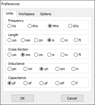
Preferences in AN-SOF allow users to customize the unit system for input and output data, adjust the workspace appearance, and configure various miscellaneous options. To access preferences, navigate to Tools > Preferences from the main menu.
Units
On the Units page of the Preferences dialog box (see Fig. 1), users can select suitable units for frequencies, lengths, wire cross-section, inductances, and capacitances. Apart from standard SI units, options such as inches (in) and feet (ft) are available for lengths and cross-sections.
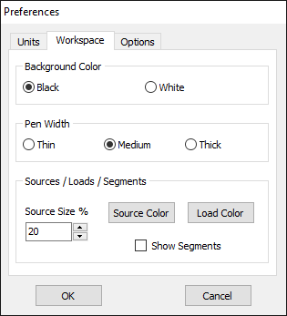
Workspace
In the Workspace tab (Fig. 2), users can toggle the workspace background color between black and white. Additionally, there are three levels for the pen width used to draw objects on the workspace: Thin, Medium, and Thick. This option applies to axes, wires, and wire grids. Users can also customize the size and color of source symbols and loads. Enabling the Show Segments option displays the segments in the workspace.
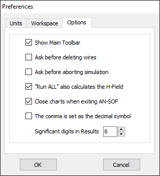
Options
In the Options tab, users can check the Show Main Toolbar option to display the toolbar (Fig. 3). Two “Ask before…” questions can be set to avoid mistakes. If the option “Run ALL” also calculates the H-Field is checked, the near H-field will be calculated after clicking on the “Run ALL” button. Users can also choose to close the chart windows after exiting AN-SOF. Additionally, the option “The comma is set as the decimal symbol” should be selected if the comma is used as the decimal separator in the Windows® regional settings. Users can also set the number of significant digits shown in results, although this option does not modify the double precision used in the internal algorithms.
Note
All preferences can be configured at any time, either before or after performing a calculation.
Display Options
The workspace background can be set to white or black. When a white (black) background is chosen, all wires will default to black (white) unless a different color is specified for specific wires. To set the workspace color, navigate to Tools > Preferences > Workspace tab. The color of selected wires can be changed at any time via Edit > Wire Color in the main menu.
The line width used for drawing wires and axes in the workspace can be adjusted by selecting a Pen Width option in the Workspace tab of the Preferences dialog box. There are three levels: Thin, Medium, and Thick. Figure 1 illustrates the different combinations of workspace color and pen width that can be achieved.
Viewing 3D Axes
To customize the appearance of the X, Y, Z axes in the workspace, navigate to View > Axes (Ctrl + A) in the main menu to open the Axes dialog box (see Fig. 2). There are two types of axes:
- Small Axes: Displayed in the lower-left corner of the workspace.
- Main Axes: Displayed at the center of the screen.
Both positive and negative axes can be displayed. The color of the main axes can be changed by clicking the Color button. Check the Show Ticks option to add a specified number of ticks to the Main Axes.
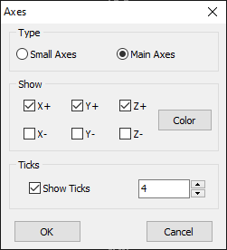
Tip
Press F7 to switch between small and main axes.
Zooming the View
To zoom in or out of the structure in the workspace:
- Use the mouse wheel.
- On a laptop touchpad, use two fingers (similar to zooming an image).
- Alternatively, use the Zoom In (Ctrl + I) and Zoom Out (Ctrl + K) commands in the View menu.
For a more specific zoom on a particular area, click the Zoom (magnifying glass) button on the toolbar and drag a rectangle over the desired area. To return to the initial view, click the Initial View (Home) button on the toolbar.
Rotating the View
To rotate the view of the structure around a specific axis:
- Press one of the following toolbar buttons:
- Rotate around X
- Rotate around Y
- Rotate around Z
- 3D Rotation
- Move the mouse while holding the left button.
Alternatively, use the following keyboard shortcuts:
- F1: Right-handed rotation around the x-axis.
- F2: Left-handed rotation around the x-axis.
- F3: Right-handed rotation around the y-axis.
- F4: Left-handed rotation around the y-axis.
- F5: Right-handed rotation around the z-axis.
- F6: Left-handed rotation around the z-axis.
Moving the View
To move the view of the structure in the workspace:
- Click the Move button on the toolbar.
- Move the mouse while holding the left button.
Introduction
The Method of Moments (MoM) is widely recognized as one of the most reliable techniques for modeling and simulating antennas and radiating systems. However, traditional implementations of MoM suffer from several issues primarily stemming from approximations used in numerical calculations to reduce computational requirements. While these approximations were justified in the 1970s and 1980s due to limited processor speeds and memory capacities, the present-day computing power, even on personal computers, allows for more accurate calculations. The limitations imposed by these approximations in traditional MoM models restrict their validity and applicability.
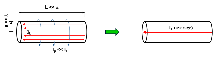
The fundamental principle of MoM involves representing metal surfaces through wire segments, which is a suitable approximation for many metallic antennas, particularly wire-type antennas like linear antennas, dipoles, monopoles, yagis, log-periodic arrays, quads, antenna arrays of all types, traveling wave antennas, fractals, aperture antennas, and reflectors. It is essential for each wire segment to have a small length and cross-section relative to the wavelength. The MoM seeks to determine the unknown current flowing through each wire segment, as depicted in Fig. 1.
The Thin-Wire Approximation
In the modeling of antennas using cylindrical wire segments, the initial approximation commonly employed is known as the “thin-wire approximation,” as illustrated in Fig. 2. This approximation is based on the following assumptions:
- The electric current flowing through a wire can be represented as a filament along the wire axis, disregarding the fact that it actually flows on the wire’s surface.
- Variations in the current along the circular contour of the wire’s cross-section can be ignored.
- The component of the current perpendicular to the wire axis can be disregarded.
- It is sufficient to enforce the boundary condition of zero total tangential electric field on the surface of an ideal conducting wire along its axis.
When dealing with a wire segment with a cross-section significantly smaller than the wavelength, assumptions 2, 3, and 4 are reasonably valid and align with experimental observations and theoretical predictions in the quasi-electrostatic regime for metal surfaces. However, assumption 1, regarding the current filament along the wire axis, has sparked debates throughout the history of linear antennas.
Assumption 1 only holds as a limiting case when the wire’s cross-section approaches zero size, such as when the wire has a circular cross-section and its radius tends to zero. This assumption relates to the crucial aspect known as the Kernel of the problem. The Kernel represents the core of the integral equation that the MoM solves to determine the currents flowing along the wires. Instead of employing the “thin-wire Kernel” utilized in traditional MoM, which is based on assumption 1, AN-SOF employs the exact Kernel. In the exact Kernel, it is considered that the current flows on the surface of the wires rather than being confined to a filament along the wire axis.
Eliminating assumption 1 has a significant impact on the accuracy of calculations, particularly in the current distribution near the antenna’s feed point or terminals, where obtaining precise values for input impedance and standing wave ratio (SWR) is crucial. In addition to discarding assumption 1 in AN-SOF, the use of the exact Kernel and curved wire segments helps overcome other issues inherent in traditional MoM, as described below.
Overcoming the 7 Limitations of the Traditional MoM
In AN-SOF, we have departed from the traditional MoM and embraced innovation by implementing a new method called the Conformal Method of Moments (CMoM) with an exact Kernel formulation. This decision stems from the lack of substantial improvements in traditional methods over several decades, despite advancements in computational power. By adopting CMoM with an exact Kernel, we have successfully addressed the main limitations of the traditional MoM, which can be categorized into seven key areas:
1. No curved wires:
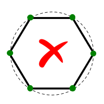
Traditional MoM models rely on straight wire segments, which are suitable for linear antennas such as dipoles and their arrays. However, many antennas and structures have curved shapes. In traditional MoM, curved wires are approximated using a series of straight-line segments, leading to modeling errors that persist throughout the simulation. This approximation often produces inaccurate results for curved antennas like loops, helices, and spirals, particularly in terms of feed point impedances.
2. Wire spacing limitation:
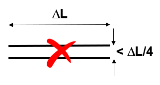
Another limitation of traditional MoM is the spacing between parallel wires. Misleading results occur when the spacing between segments is less than a quarter of the segment length. As a result, the traditional MoM becomes less applicable when modeling configurations with close parallel wires, such as in two-wire transmission lines.
3. Issues with bent wires:
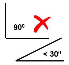
The thin-wire Kernel employed in traditional MoM leads to erratic numerical oscillations when wires are bent at right angles or have angles less than 30 degrees between adjacent segments.
4. Short segment constraint:
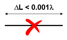
Traditional MoM imposes a constraint on the segment length, requiring it to be greater than 0.001 of a wavelength. Consequently, the traditional MoM cannot be effectively applied at very low frequencies. For instance, when modeling an electric circuit of around 1 meter operating at 60 Hz, the segment length needed to accurately represent the circuit becomes at least 5,000 times shorter than the minimum segment length supported by traditional MoM. Therefore, the traditional MoM implementation falls short when modeling wire antennas at low frequencies.
5. Thin wire requirement:
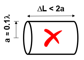
Thick wires deviate from the thin-wire approximation assumption, where current flow is limited to the wire axis rather than its surface. This deviation introduces significant errors in the results.
6. Tapered wire issues:
Changes in radius between adjacent segments create non-physical discontinuities in traditional MoM simulations.

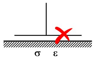
7. Proximity to lossy ground plane affects horizontal wires:
Antennas such as monopoles positioned above ground screens with elevated radial wires exhibit diverging input impedance and inaccurate antenna efficiency due to the influence of the lossy ground plane.
Thanks to the Conformal Method of Moments (CMoM) with Exact Kernel, AN-SOF has successfully eliminated these limitations. CMoM employs conformal segments that accurately capture the structure’s contour, enabling an exact representation of geometric details. Conformal segments, resembling curved cylindrical tubes, enable precise modeling of curved wires. By employing the exact Kernel instead of the thin-wire approximation, AN-SOF overcomes limitations associated with bent wires, small wire spacings, and segment lengths. This approach facilitates highly accurate calculations compared to the traditional method.
With the implementation of CMoM and an exact Kernel formulation, AN-SOF achieves enhanced accuracy, reduced computational requirements, and more efficient simulations. The improved method enables AN-SOF to simulate a wide frequency range, spanning from extremely low frequencies (e.g., 60 Hz circuits) to microwave antennas.
AN-SOF stands as the only antenna modeling software that offers a calculation engine based on the Conformal Method of Moments with an Exact Kernel.
Simulation Setup
Before drawing wires or running a simulation, it’s recommended to configure the simulation parameters in the Setup tab. This tab contains the following panels: Frequency, Environment, Far-Field, Near-Field, Excitation, and Settings (see Fig. 1).
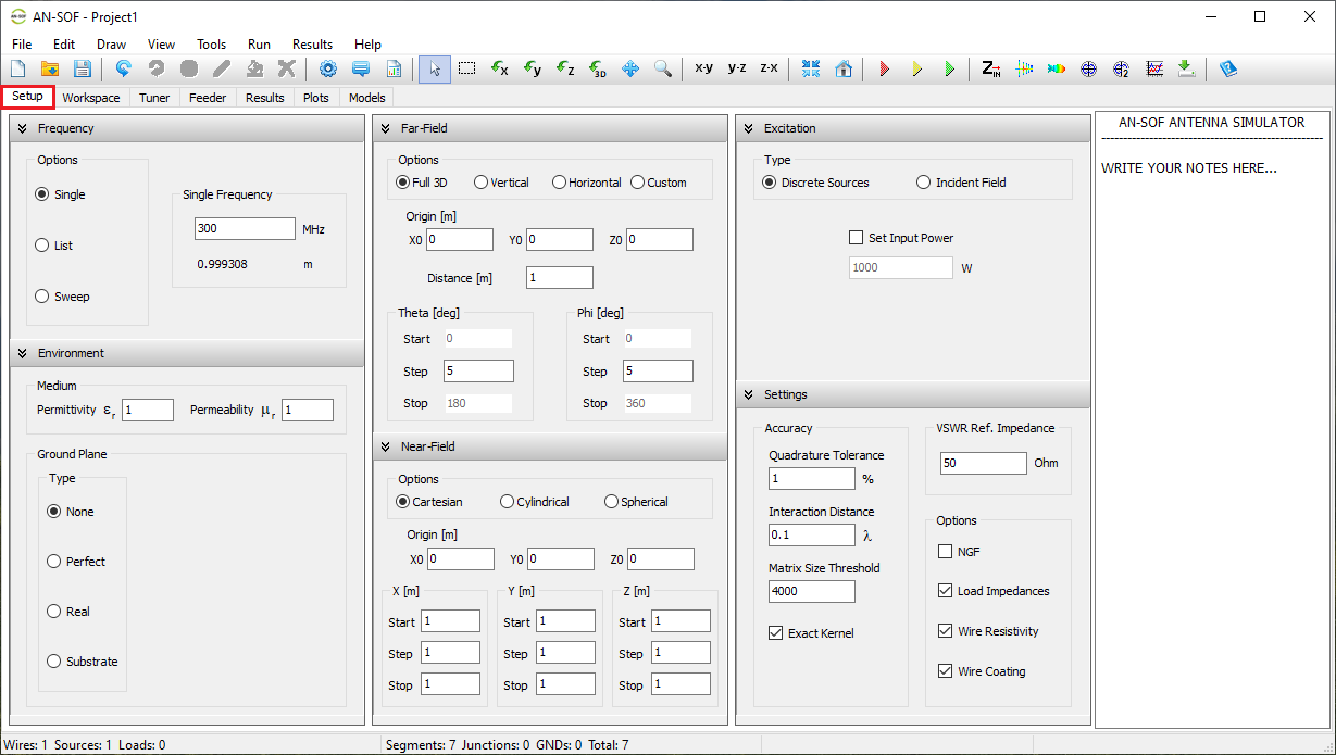
- Frequency panel: Specify the operating frequencies for the project.
- Environment panel: Set the relative permittivity and permeability of the surrounding medium, as well as the ground plane type.
- Far-Field panel: Define the angular ranges for far-field calculations.
- Near-Field panel: Define the observation points for near-field calculations.
- Excitation panel: Choose the excitation type for the structure. If using discrete sources, set the total input power. If using an incident field, define its direction and polarization.
- Settings panel: Set the reference impedance for VSWR and adjust parameters to fine-tune calculation accuracy.
Additionally, a Note panel on the right side of the Setup tab allows you to add project-related notes. These notes are saved in a .txt file in the same folder as the project file, using the same filename.
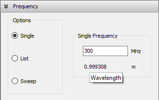
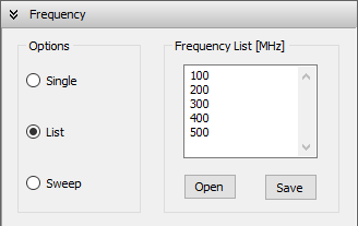
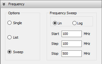
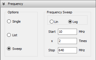
To define the operating frequencies, go to the Setup tab in the main window and select the Frequency panel. You can choose from three frequency modes: Single, List, or Sweep.
- Single: Enter a single frequency value in the Single Frequency box (see Fig. 1). The corresponding wavelength is displayed automatically below the frequency field.
- List: Enter multiple frequencies in the Frequency List box (Fig. 2). You can import a list from a text file using the Open button, or export the current list using the Save button.
- Sweep: Perform a frequency sweep using either a linear or logarithmic scale.
- For a linear sweep, specify the start, step, and stop frequencies (Fig. 3).
- For a logarithmic sweep, enter the start and stop frequencies, along with a multiplication factor (Fig. 4).
To change the frequency unit (e.g., Hz, kHz, MHz, GHz), go to Tools > Preferences in the main menu, and select the desired unit on the Units page of the Preferences dialog box. See Preferences for more details.
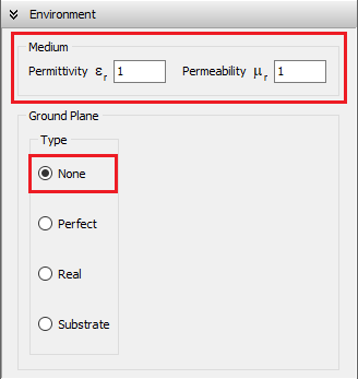
Environment and Ground Plane Options
The environment surrounding an antenna or metallic structure can be either free space or include a ground plane. In the case of free space, you can define the relative permittivity (dielectric constant εr) and magnetic permeability (µr) of the medium, with vacuum corresponding to εr = 1 and µr = 1.
Three ground plane options are available:
- Perfect Electric Conductor (PEC): An ideal, lossless ground plane.
- Real (Lossy) Ground: A ground plane with user-defined conductivity (σ) and relative permittivity (εr). Optionally, a radial ground screen can be added.
- Dielectric Substrate Slab: Used for modeling microstrip lines and printed antennas.
All ground planes lie in the xy-plane. The available environment settings will be described in detail in the sections below.
Configuring the Medium Properties
To configure the medium, navigate to the Setup tab > Environment panel. Use the Medium box (Fig. 1) to set the relative permittivity (εr) and permeability (µr) of the surrounding medium. When a ground plane is used, these values represent the permittivity and permeability of the medium above the ground.
Note:
The wavelength displayed below the frequency set in the Frequency panel (when the Single option is selected) and the wavelength used internally by AN-SOF for calculations will be adjusted based on the specified permittivity and permeability of the medium. Specifically, these properties cause the wavelength to shorten accordingly relative to the wavelength in a vacuum.
None (Free Space)
Selecting the None option simulates the antenna in free space. The relative permittivity (εᵣ) and permeability (µᵣ) specified in the Medium box (see Fig. 1) define the properties of the surrounding environment.
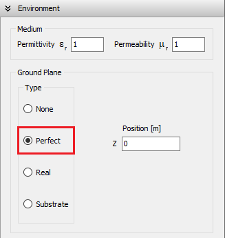
Perfect (PEC Ground)
Selecting the Perfect option places an infinitely large, perfectly electrically conducting (PEC) ground plane at a specified height relative to the xy-plane (see “Z Position” in Fig. 2). The ground plane remains parallel to the xy-plane, and its position is defined by the Z coordinate: a negative Z places the ground plane below the xy-plane, while a positive value places it above.
When using a perfect ground plane, all wires must be located above it—that is, each wire must have a Z-coordinate greater than or equal to the specified ground plane position. Wires crossing through or lying below the ground plane are not allowed. Additionally, horizontal wires placed directly on the ground plane are unsupported. However, connections from wire ends to the ground plane are permitted.
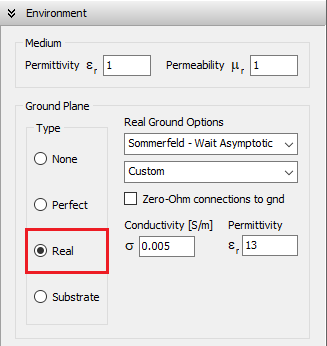
Real (Lossy Ground)
Selecting the Real option places a lossy ground plane at the xy-plane (z = 0), with user-defined conductivity (σ) and relative permittivity (εᵣ), as shown in Fig. 3. Four modeling methods are available for real ground calculations:
- Sommerfeld–Wait
- Reflection Coefficients
- Radial Wire Ground Screen
- Sommerfeld–Norton
These options are described in the following sections.
All wires must be positioned above the ground plane (z > 0). Horizontal wires directly on the ground plane are not supported.
Wire end connections to the ground are allowed when using either the Sommerfeld–Wait or Radial Wire Ground Screen options.
The Reflection Coefficients and Sommerfeld–Norton models assume perfect (zero-Ohm) wire connections to ground and yield reasonable results only for vertical wires connected to good conducting grounds—not dielectric surfaces. These models are not suitable when vertical wire-to-ground connections are made through dielectric materials.
Real Ground: Sommerfeld – Wait
This option models the antenna/wire currents using a hybrid approach that combines a perfect ground plane with loss impedances to account for power dissipation in the real ground—particularly important when wires are close to or connected to the ground. Developed by Prof. James R. Wait, this model is especially effective for low-frequency (LF) and medium-frequency (MF) antennas, where ground conductivity tends to be high. However, it remains applicable at higher frequencies as long as the ground behaves as a good conductor.
The model uses the ground’s conductivity (σ) and permittivity (εᵣ) to compute both near-field and far-field radiation, applying Norton’s asymptotic approximations to the exact Sommerfeld solution. The far-field results match those predicted by Fresnel reflection coefficients.
Wire connections to ground are supported. If a wire’s starting or ending point is located at z = 0, it will automatically be connected to the ground. These connections are treated as imperfect (lossy) by default, meaning power can be dissipated at the connection point due to current flow. If the Zero-Ohm connections to ground option is enabled, these connections are instead treated as perfect (lossless), though the presence of the lossy ground still influences the overall near and far fields.
In summary, the Sommerfeld – Wait model is appropriate when the ground can be considered a good conductor at the operating frequency and when the structure includes wire-to-ground connections.
Real Ground: Reflection Coefficients
When this option is selected, the ground conductivity (σ) and relative permittivity (εᵣ) influence the current distribution on the antenna or wire structure above the ground. As a result, the input impedance of a transmitting antenna is also affected by real ground conditions. This influence is determined using a generalization of Fresnel’s reflection coefficients, which is theoretically valid when wires are positioned several wavelengths above the ground. In practice, however, good results have been reported for heights between one-quarter and one-half of a wavelength.
Near fields are calculated using Norton’s asymptotic approximations to Sommerfeld’s exact solution, allowing the electric and magnetic fields to be computed as a function of distance from the antenna. This enables analysis of field attenuation due to ground losses. The far field, by contrast, is computed using the standard Fresnel reflection coefficients.
Vertical wire connections to ground may be added when the ground behaves as a good conductor at the operating frequency, even though these connections theoretically violate the height requirement. These wire-to-ground connections are treated as lossless in this model.
In summary, the Reflection Coefficients ground model is best suited for wire structures located several wavelengths above ground, ideally without any wire-to-ground connections. However, if the ground is a good conductor at the operating frequency, vertical wire connections may be included—but results under such conditions should be interpreted with caution.
Real Ground: Radial Wire Ground Screen
When this option is selected, a ground screen made of buried radial wires is placed on the ground plane, which has the specified conductivity (σ) and relative permittivity (εᵣ). The screen is centered at the origin (0,0,0), and its configuration is defined by user-specified parameters: the number of radial wires, their length (or screen radius), and wire radius. These wires are assumed to be laid on the ground surface or buried at a depth less than one soil skin depth.
This model is based on Prof. James R. Wait’s theory for good conducting grounds. It affects the current distribution on the antenna or wire structure by accounting for the power dissipated in the combined ground plane and wire screen system. As a result, both the presence of the screen and the ground properties (conductivity and permittivity) influence the input impedance of a transmitting antenna located above the screen. The same parameters are used to compute the radiated near and far fields using Norton’s asymptotic approximations to Sommerfeld’s solution and Fresnel reflection coefficients, respectively.
Wire-to-ground connections may be defined at wire endpoints located at z = 0. These are treated as imperfect by default, meaning that power is dissipated in the ground-screen system due to currents flowing between the ground and the wires. If the Zero-Ohm connections to ground option is enabled, these connections are treated as perfect, with no power dissipation at the contact point.
In summary, the Radial Wire Ground Screen model is suitable when the ground behaves as a good conductor at the operating frequency and when the structure includes wire-to-ground connections. The screen serves to increase the effective conductivity of the combined ground-screen system, reducing power losses beneath antennas placed above it. Typical use cases include monopole antennas in the form of poles or radiating towers used in broadcasting applications.
Real Ground: Sommerfeld – Norton
Unlike the previous ground models, which apply various approximations to compute the current distribution on wires above a lossy ground plane, the Sommerfeld–Norton model numerically solves Sommerfeld’s exact solution. This enables simulations where the ground does not need to be a good conductor—it may instead be a dielectric medium. To approximate a purely dielectric ground, enter a very low conductivity (e.g., σ = 1E-6 S/m) along with the desired relative permittivity (εᵣ).
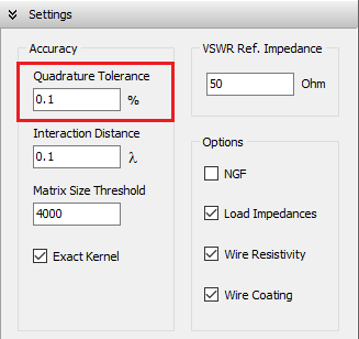
Vertical wires can be placed very close to the ground, with a minimum height of one wire radius above ground. Horizontal wires can be simulated as low as 0.005λ above ground. For vertical or horizontal wires at heights below 0.01λ, it is important to increase the accuracy of the calculations. To do this, go to Setup tab > Settings panel and set the Quadrature Tolerance to 0.1%, instead of the default 1% (see Fig. 4).
The near fields are computed from the current distribution using Norton’s asymptotic approximation to Sommerfeld’s solution. This is accurate at distances greater than about one-quarter wavelength from the wire structure, which is sufficient for most practical applications. The far field, in contrast, is calculated using Fresnel reflection coefficients, which yield the correct asymptotic expressions.
Wire-to-ground connections are theoretically not permitted in this model. However, they can be used with caution only for vertical wires, and only if the ground behaves as a good conductor at the operating frequency. In such cases, the model assumes lossless connections and employs specular reflection of the fields to compute the current distribution. These assumptions are valid only when the ground is effectively conductive.
In summary, the Sommerfeld–Norton model is the most accurate among the available ground models, but it comes with certain restrictions. It is recommended for highly dielectric grounds or situations where the ground cannot be considered a good conductor. Horizontal wires must not be placed below 0.005λ above ground. Vertical wires may be connected to ground only when the ground is a good conductor, and the results in such cases should be interpreted with care.
Interactive Ground Model Selection Tools
To assist in selecting the appropriate real ground model, you can access the Loss Tangent Calculator and Ground Plane Selector here:
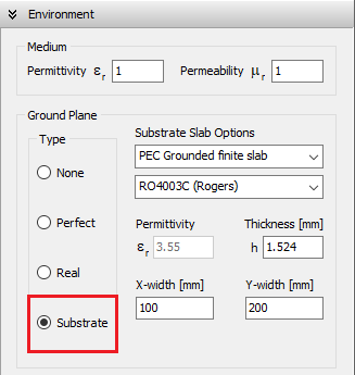
Substrate (Grounded Dielectric Slab)
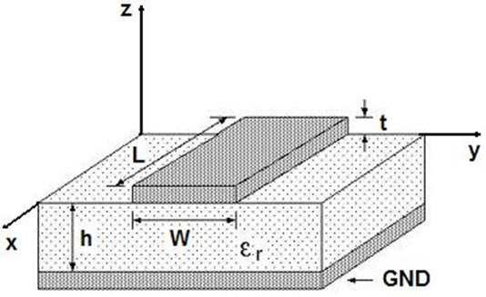
When this option is selected, a dielectric substrate with user-defined relative permittivity (εᵣ) is placed beneath the xy-plane (z = 0), as shown in Figs. 5 and 6. The slab may extend infinitely or have finite dimensions in the xy-plane, where you can define its width along the X and Y directions. The substrate thickness, denoted as h, must also be specified. A perfectly electrically conducting (PEC) ground plane is located at z = –h, just below the dielectric slab (see Fig. 6). A drop-down list is available to select common substrate materials (e.g., FR4, RT/Duroid, Rogers RO). Note that the dielectric loss tangent cannot be specified—it is assumed to be zero, meaning the substrate is treated as lossless.
When the Substrate option is active:
- All wires must lie horizontally in the xy-plane (z = 0). These wires typically represent traces of printed antennas, microstrip lines, or PCB tracks.
- The only exception is for vertical wires (vias), which may connect traces at z = 0 to the ground plane at z = –h. These are commonly used to feed the structure with voltage or current sources.
Important constraints:
- The PEC ground plane beneath the substrate is mandatory and cannot be omitted. As a result, ungrounded dielectric substrates are not supported.
- Wires above the xy-plane (z > 0) or below the ground plane (z < –h) are not allowed in this model.
The Substrate model is an extension of the Conformal Method of Moments tailored for printed wire structures. It has the following limitations:
Model Limitations
Single-Layer, Lossless Substrate Only
- Only one dielectric layer is supported (multilayer stacks are not).
- The substrate must be lossless (loss tangent is assumed to be zero).
- No holes or cutouts are permitted in the substrate.
Finite-Size Substrate Constraints
- The substrate must be rectangular in shape.
- Traces must be placed at least 5× their width away from the substrate edges.
Ground Plane and Vias
- A PEC ground plane is always present and cannot be disabled.
- Vertical wires (vias) can be added to connect traces to the ground, typically for feeding.
No Slot-Based Designs
- Slot antennas or patches with slots cannot be modeled due to software limitations.
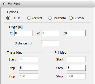
To configure radiation pattern parameters, navigate to the Setup tab in the main window and select the Far-Field panel (Fig. 1).
The far field can be computed after calculating the current distribution. Thus, the parameters set in the Far-Field panel have no effect on the determination of the currents and can be modified at any time. However, the far field must be recalculated every time these parameters are modified.
There are four options for radiation pattern calculations:
Full 3D
The far field is calculated in angular ranges that cover the entire 3D space, allowing you to obtain 3D radiation lobes. The steps for the Theta (zenith) and Phi (azimuth) angles can be set in the Theta [deg] and Phi [deg] boxes.
Vertical
The far field is calculated at a vertical slice for a given Phi (azimuth) angle. The step for the Theta (zenith) angle can be set in the Theta [deg] box, while the fixed Phi can be set in the Phi [deg] box.
Horizontal
The far field is calculated at a horizontal slice for a given Theta (zenith) angle. The step for the Phi (azimuth) angle can be set in the Phi [deg] box, while the fixed Theta can be set in the Theta [deg] box.
Custom
The far field is calculated for the specified ranges of angles Theta (zenith) and Phi (azimuth). The start, step, and stop values for Theta and Phi can be set in the Theta [deg] and Phi [deg] boxes.
Additionally, the following parameters can be set:
Origin (X0,Y0,Z0)
This is any point used as a phase reference. Its coordinates do not affect the shape of the radiation pattern. The 3D radiation pattern will be plotted centered at this point.
Distance
This represents the distance from (X0,Y0,Z0) to an observation point in the far-field region. A normalized far-field pattern can be obtained by setting Distance = 1 meter.
The zenith and azimuth angles, Theta (θ) and Phi (ɸ), are shown in Fig. 2. The figure also illustrates the Distance R from the structure to an observation point in the far-field zone. These three numbers (R, θ, ɸ) define the spherical coordinates of the far-field point.
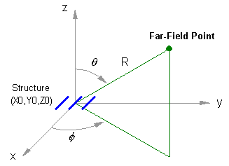
A frequently asked question is how to displace the center of the radiation pattern in a 3D plot displaying the radiation lobes. The answer lies in setting the Origin (X0, Y0, Z0) in the Far-Field panel. This allows you to adjust the reference point for the radiation pattern, enabling better visualization of the results. For more details, refer to this article:
To configure the observation points for the calculation of near fields, navigate to the Setup tab in the main window and select the Near-Field panel.
The near field can be computed after calculating the current distribution. Thus, the parameters set in the Near-Field panel have no effect on the determination of the currents and can be adjusted at any time. However, the near field must be recalculated whenever these parameters are modified.
The Near-Field panel provides three coordinate system options for near-field calculations:
- Cartesian
- Cylindrical
- Spherical
By selecting one of these options, near fields can be calculated in Cartesian, Cylindrical, or Spherical coordinates, depending on your preference or the requirements of your analysis.
Cartesian Coordinates
If the Cartesian option is selected, the following parameters can be configured for near-field calculations (Fig. 1):
Origin (X0, Y0, Z0)
This is the origin of the Cartesian coordinate system used to define the observation points where near fields will be calculated.
X
This box is used to specify the x-coordinates of the observation points where near fields will be calculated. You must set the start, step, and stop values for the x-coordinates. The start and stop values are measured relative to X0.
Y
This box is used to specify the y-coordinates of the observation points where near fields will be calculated. You must set the start, step, and stop values for the y-coordinates. The start and stop values are measured relative to Y0.
Z
This box is used to specify the z-coordinates of the observation points where near fields will be calculated. You must set the start, step, and stop values for the z-coordinates. The start and stop values are measured relative to Z0.
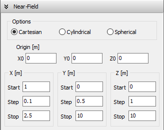
Cylindrical Coordinates
If the Cylindrical option is selected, the following parameters can be configured for near-field calculations (Fig. 2):
Origin (X0, Y0, Z0)
This is the origin of the cylindrical coordinate system used to define the observation points where near fields will be calculated.
R
This box is used to specify the radial distances (R-coordinates) of the observation points where near fields will be calculated. You must set the start, step, and stop values for the radial distances. The start and stop distances are measured relative to the origin (X0, Y0, Z0).
Phi
This box is used to specify the azimuth angles (phi-coordinates) of the observation points where near fields will be calculated. You must set the start, step, and stop values for the azimuth angles in degrees.
Z
This box is used to specify the z-coordinates of the observation points where near fields will be calculated. You must set the start, step, and stop values for the z-coordinates.
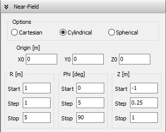
Spherical Coordinates
If the Spherical option is selected, the following parameters can be configured for near-field calculations (Fig. 3):
Origin (X0, Y0, Z0)
This is the origin of the spherical coordinate system used to define the observation points where near fields will be calculated.
R
This box is used to specify the radial distances (R-coordinates) of the observation points where near fields will be calculated. You must set the start, step, and stop values for the radial distances. The start and stop distances are measured relative to the origin (X0, Y0, Z0).
Theta
This box is used to specify the zenith angles (theta-coordinates) of the observation points where near fields will be calculated. You must set the start, step, and stop values for the zenith angles in degrees.
Phi
This box is used to specify the azimuth angles (phi-coordinates) of the observation points where near fields will be calculated. You must set the start, step, and stop values for the azimuth angles in degrees.
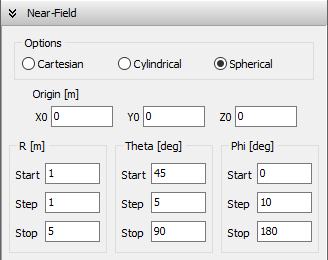
Near-Field Calculation Workflow
The Cartesian, Cylindrical, and Spherical options described above define a grid of observation points where the near field will be computed. The near electric field (E-field) and near magnetic field (H-field) can be calculated separately, or you can compute them sequentially by clicking Run Currents and Near-Field (F11) in the Run menu or toolbar. This command first calculates the current distribution and then computes the near fields.
Alternatively, the calculation of the current distribution, far-field, and near-field can be executed in a single step by selecting the Run ALL (F12) command in the Run menu.
If the near H-field is not required, you can disable its automatic calculation by turning off the “Run ALL also calculates the H-Field” option. This setting can be found in the Options tab of the Preferences window. To access the Preferences window, click the gear button in the main toolbar or navigate to Tools > Preferences in the main menu.
⚠ Note:
When defining the grid of points for near-field calculations, the closest distance from a near-field point to a wire with a circular cross section must be at least five times the wire radius. For flat strip conductors (such as those used in metallic surfaces), the near-field point must be located at a distance of at least one strip width from the strip.
Accessing Excitation Settings
Navigate to:
Setup tab > Excitation panel
Two excitation types available (Fig. 1):
- Discrete Sources
- Incident Field
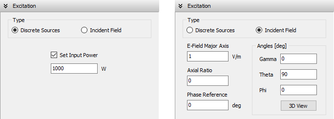
Discrete Sources
- Purpose: Calculate current distribution using voltage/current sources on wires
- Power Configuration:
- Specified Input Power: Sources auto-adjust to achieve target power (Watts)
- Unspecified Power: Sources remain constant; power becomes output result
Incident Field (Plane Wave Excitation)
Define an incident plane wave’s direction and polarization:
Key Parameters
| Parameter | Description | Units/Values |
|---|---|---|
| E-Field Major Axis | Linear: RMS amplitude (V/m) Elliptical: Major axis of polarization ellipse | V/m |
| Axial Ratio | Minor/major axis ratio: – Positive: Right-handed ellipse – Negative: Left-handed ellipse – Zero: Linear polarization | Unitless |
| Phase Reference | Phase shift at coordinate origin | Degrees |
| Gamma | Linear: Polarization angle from incidence plane Elliptical: Major axis angle from incidence plane | Degrees |
| Theta | Zenith angle of incidence | Degrees |
| Phi | Azimuth angle of incidence | Degrees |
3D Visualization
Click 3D View (Fig. 3) to interactively set:
- Wave direction
- Polarization state
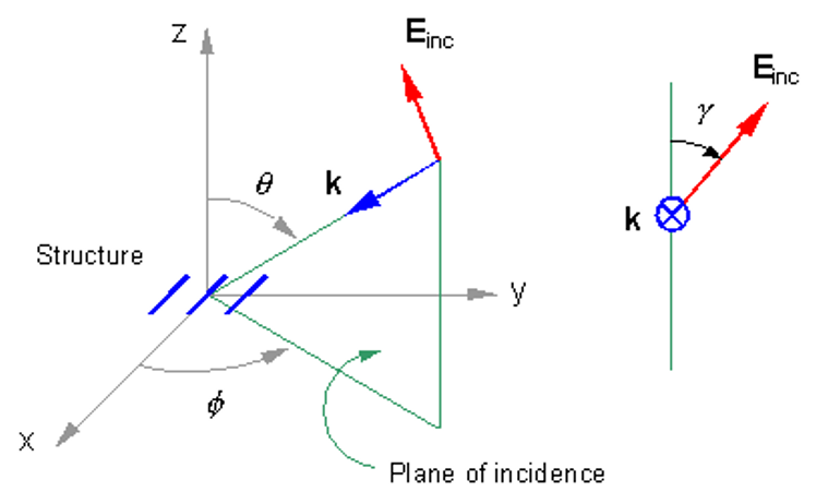
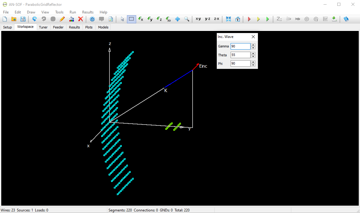
Note
When an incident plane wave is used as the excitation, any discrete sources present will be ignored during the simulation.
Note
When an incident plane wave is used as the excitation, the calculated far-field and near-field results represent the scattered fields. The resulting radiation pattern is the scattered field pattern, observed in the far-field region where the scattered field amplitude decays with the inverse of the distance (1/r), and the scattered power density decays with the inverse square of the distance (1/r²) from the structure.
To access advanced simulation options, go to the Setup tab and select the Settings panel. Here, you can:
- Fine-tune the accuracy of the simulation,
- Set the reference impedance for VSWR calculations, and
- Adjust various options that affect the calculation engine.
These settings provide greater control over simulation precision and convergence behavior. See Fig. 1.
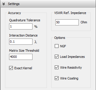
Controlling Numerical Precision
The Accuracy section in the Settings panel allows you to control the precision of the simulation and manage memory usage for large models.
- Quadrature Tolerance defines the acceptable numerical error in the evaluation of integrals between wire segments that are closer than the Interaction Distance. This parameter governs the precision of electromagnetic interaction calculations. The default value is 1%.
- Interaction Distance sets the maximum separation (in wavelengths) between segments for which the numerical integration guarantees an error below the Quadrature Tolerance. For segments farther apart than this distance, a third-degree polynomial approximation is used instead of the traditional Hertzian dipole approximation, offering improved accuracy for curved segments. The default value is 0.1λ.
- Matrix Size Threshold determines the maximum size of the impedance matrix (N × N, where N is the number of wire segments) that is computed in double precision. For models with more segments than the set threshold, single precision is used to reduce memory usage. While this may slightly reduce accuracy, it enables the simulation of larger models on systems with limited Windows on-board memory. The default threshold is 4,000.
- Exact Kernel enables the use of the exact formulation of the Electric Field Integral Equation (EFIE), significantly improving accuracy for antennas made with thicker wire segments. When this option is disabled, an extended thin-wire approximation is used. See The Exact Kernel for more information.
VSWR Reference Impedance Configuration
The reference impedance serves as the normalization value for VSWR calculations throughout the simulation. This parameter is particularly important when matching simulation conditions to real-world measurement setups.
Key features:
- Defaults to 50 Ω (standard for most RF systems)
- Commonly adjusted to 75 Ω for television/video applications
- Requires refreshing the results (Ctrl + R) to update all VSWR-dependent data
Simulation Control Options
These global toggles enable efficient comparison of different simulation scenarios without modifying individual element properties. They are especially valuable for parametric studies and troubleshooting.
| Option | Technical Implementation | Practical Application |
|---|---|---|
| NGF | Stores LU-decomposed impedance matrix after first calculation | Accelerates repeated simulations with varying source excitations |
| Load Impedances | Master switch for all lumped load elements in the model | Quickly compare loaded vs. unloaded system performance |
| Wire Resistivity | Toggles Ohmic loss calculation for all conductors | Evaluate conductor loss impact on system efficiency |
| Wire Coating | Enables/disables dielectric coating effects | Analyze insulation impact on antenna performance |
Implementation Note:
These options provide non-destructive alternatives to physically removing/readding model elements when running comparative analyses.
A summary of the project information can be displayed by navigating to View > Project Details in the main menu. This opens the Project Details window (Fig. 1). Alternatively, you can access this window using the dedicated button on the toolbar.
The text in the Project Details window can be selected and copied to the clipboard in the usual way (Ctrl + C to copy from the window and Ctrl + V to paste elsewhere).
The Project Details window provides a comprehensive summary of the following project information:
- Project Name: The name of the project.
- Date and Time: The date and time when the project was last saved.
- Structure: Includes the number of wires, sources, loads, transmission lines, and segment counts.
- Excitation: Indicates whether discrete sources or an incident field are set.
- Frequencies: Displays the frequency range configured for the simulation.
- Medium: Lists the permittivity, permeability, and wavelength (of the upper medium if a ground plane is present).
- Ground Plane: Specifies the type of ground plane and its associated parameters, if applicable.
- Far-Field Parameters: Displays settings related to far-field calculations.
- Near-Field Parameters: Shows settings for near-field calculations.
- Numerical Accuracy: Provides details about the settings employed for numerical accuracy.
- Units: Lists the units used for frequency, length, wire radius, inductance, and capacitance.
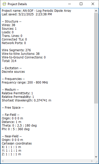
When a project is saved in AN-SOF, multiple files that share the same name as the project are saved within the same directory. Each file has a unique extension that corresponds to its specific content.
IMPORTANT: When requesting support, please compress all the project files into a ZIP archive and attach it to your support request email.
These files include:
| File type | Description |
|---|---|
| *.emm | Main file with configuration data |
| *.wre | Geometric description of the wire structure |
| *.cur | Current distribution |
| *.phi | E-phi component of the far-field. |
| *.the | E-theta component of the far-field. |
| *.pwr | Radiation pattern data |
| *.nef | Near electric field |
| *.nhf | Near magnetic field |
| *.ngf | Numerical Green’s function |
| *.txt | Notes written by the user |
Pressing ALT with the underlined letter of a menu item will execute the command associated with the item.
The following keys and associated actions are available:
| Key | Action |
|---|---|
| Home | Return the structure to the initial view |
| ESC | Deselect all wires |
| F1 | Rotate view around +X axis |
| F2 | Rotate view around -X axis |
| F3 | Rotate view around +Y axis |
| F4 | Rotate view around -Y axis |
| F5 | Rotate view around +Z axis |
| F6 | Rotate view around -Z axis |
| F7 | Show/hide main and small axes |
| F8 | Select a wire in order of creation |
| F9 | Select a wire in reverse order of creation |
| F10 | Run current distribution and far-field |
| F11 | Run current distribution and near-field |
| F12 | Run full simulation (all options) |
| Ctrl + A | Open Axes dialog box |
| Ctrl + I | Zoom in |
| Ctrl + K | Zoom out |
| Ctrl + L | Open Transmission Lines dialog |
| Ctrl + M | Modify selected wire(s) |
| Ctrl + N | Create a new project |
| Ctrl + O | Open an existing project |
| Ctrl + Q | Exit AN-SOF |
| Ctrl + R | Run current distribution only |
| Ctrl + S | Save the project |
| Ctrl + T | Open tabular input for linear wires |
| Ctrl + W | Show properties of selected wire |
| Ctrl + Y | Redo |
| Ctrl + Z | Undo |
| Ctrl + Del | Delete selected wire(s) |
| Ctrl + Ins | Show Source/Load/TL toolbar |
| Ctrl + Alt + M | Move selected wire(s) |
| Ctrl + Alt + R | Rotate selected wire(s) |
| Ctrl + Alt + S | Scale selected wire(s) |
Drawing Wires
AN-SOF provides several wire types for creating antenna geometries. Each wire type has its own geometric parameters, attributes, and material settings, which can be configured through a dedicated Draw dialog box. This dialog box allows you to insert and customize new wires directly in the workspace.
Selecting Draw from the main menu displays the following wire types:
- Line – Opens the dialog box for drawing a straight (linear) wire.
- Arc – Opens the dialog box for drawing a circular arc.
- Circle – Opens the dialog box for drawing a circular loop.
- Helix – Opens the dialog box for drawing a helical wire.
- Quadratic – Opens the dialog box for drawing a wire following a quadratic curve.
- Archimedean Spiral – Opens the dialog box for drawing an Archimedean spiral.
- Logarithmic Spiral – Opens the dialog box for drawing a logarithmic spiral.
Accessing Drawing Commands
The wire drawing tools can be accessed through any of the following:
- Main Menu → Draw
- Right-click Menu – Right-click on the workspace to open the context menu
- Main Menu → View → Drawing Panel (see Fig. 1)
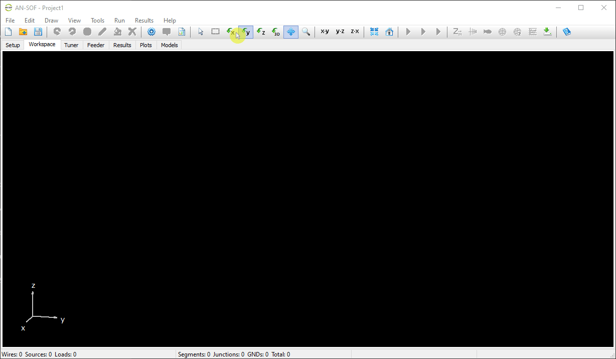
The Attributes tab is a core component of the Draw dialog box (see Fig. 1). It defines the physical and computational properties of each wire in your model, ensuring the simulation is both accurate and mathematically stable.
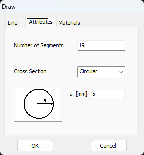
Number of Segments
To solve for the electromagnetic behavior, AN-SOF divides every wire into smaller pieces called segments. The software calculates the unknown current on each segment using the Method of Moments (MoM).
- Default Calculation: A default number is suggested based on the wire’s physical length relative to the shortest wavelength ($\lambda$) in your frequency range.
- Automatic Optimization: If you set the Number of Segments to zero, AN-SOF will automatically apply the minimum recommended density.
- Standard Rule: The automatic calculation generally targets 10 segments per wavelength (at the highest frequency) to ensure convergence and precision.
Cross-Section
Because infinitesimally thin wires do not exist in the physical world and would cause mathematical singularities, every wire must have a defined thickness.
- Available Shapes: Circular, Square, Flat, Elliptical, Rectangular, and Triangular.
- Equivalent Radius: For all non-circular shapes, AN-SOF calculates an equivalent radius. This allows the solver to treat the wire as a cylinder while maintaining the electromagnetic characteristics of the original shape (such as a flat PCB trace or a square structural member).
- Constraint: The cross-section radius or width must always be greater than zero.
Universal Application
The Attributes tab is consistent across all wire creation tools. Whether you are drawing a simple Line, an Arc, or a complex Helix, you will find these same features available to define your geometry.
In AN-SOF, the physical properties of the wire, such as the metal it is made of and whether it has insulation, are defined in the Materials tab of the Draw dialog box (Fig. 1). This allows for realistic simulations that account for ohmic losses and dielectric loading.
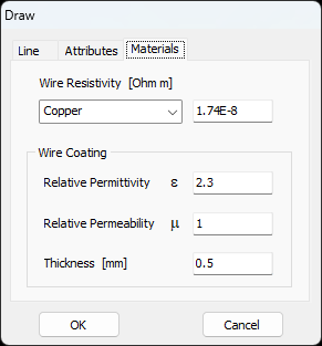
Wire Resistivity (Metallic Losses)
You can specify the resistivity ($\rho$) in $\Omega \cdot m$ to account for real-world conductor losses. AN-SOF uses this value to compute a distributed impedance per unit length, which includes the skin effect, where current tends to flow on the outer surface of the conductor at high frequencies.
Common Metals in AN-SOF:
| Material (Metals) | Resistivity [Ω m] |
| Aluminum (Pure) | 2.65E-8 |
| Aluminum (6061-T6) | 4.01E-8 |
| Aluminum (6063-T832) | 3.25E-8 |
| Brass | 6.41E-8 |
| Carbon Steel | 1.67E-7 |
| Constantan | 4.42E-7 |
| Copper | 1.74E-8 |
| German Silver | 3.33E-7 |
| Germanium | 4.55E-7 |
| Gold | 2.44E-8 |
| Iron | 9.71E-8 |
| Manganin | 4.41E-7 |
| Nichrome | 1.00E-6 |
| Nickel | 6.90E-8 |
| Phosphor Bronze | 1.10E-7 |
| Silver | 1.59E-8 |
| Solder | 1.43E-7 |
| Stainless Steel | 9.09E-7 |
| Stainless Steel 302 | 7.19E-7 |
| Tin | 1.14E-7 |
| Tungsten | 5.49E-8 |
| Zinc | 5.90E-8 |
- Custom: Manually enter a value for materials not listed.
- Perfect (PEC): Sets the wire as a Perfect Electrical Conductor (zero loss).
⚠️ IMPORTANT: To include these losses in your simulation, ensure the Wire Resistivity option is checked in the Settings panel of the Setup tab.
Wire Coating (Insulation)
If your antenna uses insulated wires, you can define the dielectric coating. AN-SOF assumes a circular cross-section for the coating.
Coating Parameters:
- Relative Permittivity ($\varepsilon_r$): The dielectric constant of the insulation (e.g., ~2.3 for polyethylene).
- Relative Permeability ($\mu_r$): The magnetic constant of the coating (usually 1.0 for non-magnetic insulators).
- Thickness: The physical depth of the coating layer. Set to 0 if the wire is bare.
⚠️ IMPORTANT: To account for the velocity factor and loading effects of the insulation, ensure the Wire Coating option is checked in the Settings panel of the Setup tab.
Geometry Note
For wires with non-circular cross-sections (like flat strips), AN-SOF utilizes an equivalent radius calculation to determine the metallic impedance behavior.
In AN-SOF, you can globally control whether the software accounts for metallic losses or treats the entire structure as a Perfect Electric Conductor (PEC). This is a powerful feature for benchmarking, as it allows you to quickly compare the idealized performance of your antenna against its real-world performance with ohmic losses.
How to Toggle Resistivity
Instead of manually editing every wire in your model, use the global toggle:
- Navigate to the Setup tab in the main AN-SOF window.
- Locate the Settings panel (Fig. 1).
- To Enable Losses: Check the Wire Resistivity box. AN-SOF will now use the specific resistivity values (e.g., for copper or aluminum) you assigned to each wire in the Draw dialog.
- To Disable Losses: Uncheck the Wire Resistivity box. The software will ignore all individual wire resistivity settings and treat every conductor as having zero resistance (PEC).
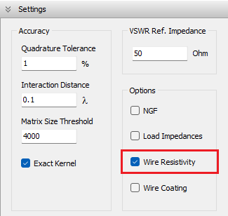
Why Use This Toggle?
- Efficiency Analysis: Running a simulation twice, once with resistivity enabled and once without, provides a clearer understanding of how ohmic losses affect the antenna’s radiation efficiency.
- Troubleshooting: If your antenna’s gain is lower than expected, disabling resistivity helps you determine if the issue is due to high ohmic losses or poor impedance matching.
- Fast Prototyping: Use the PEC (disabled) setting during the initial design phase to speed up optimization before adding the complexity of skin-effect losses.
Similar to the resistivity toggle, AN-SOF provides a global master switch for wire insulation. This allows you to quickly assess the velocity factor and dielectric loading effects of your coating without having to manually remove the insulation from every wire in your model.
How to Toggle Coating
To switch between bare wires and insulated wires:
- Navigate to the Setup tab in the main AN-SOF window.
- Locate the Settings panel (Fig. 1).
- To Enable Insulation: Check the Wire Coating box. AN-SOF will apply the permittivity, permeability, and thickness values you assigned in the Materials tab of the Draw dialog.
- To Disable Insulation: Uncheck the Wire Coating box. The software will treat all wires as bare conductors, effectively setting the coating thickness to zero for the entire simulation.
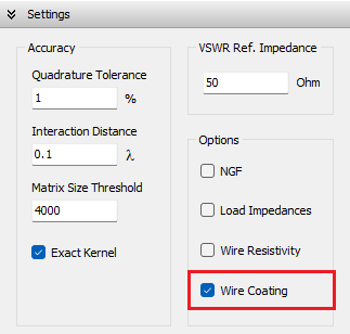
Technical Impact
- Resonant Frequency: Insulation typically increases the capacitance of the wire, lowering the resonant frequency. By toggling this setting, you can see exactly how much the insulation “electrically lengthens” your antenna.
While AN-SOF is based on wire modeling, it allows you to simulate structures with various physical cross-sections. This is achieved by calculating an equivalent radius: the radius of a circular wire that would produce the same average electromagnetic fields as the actual shape.
You can select the cross-section type from the Attributes page of the Draw dialog box (Fig. 1).
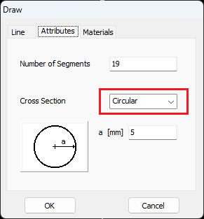
Cross-Section Types and Formulas
AN-SOF provides six geometry options, automatically converting them to an equivalent radius $a_{eq}$ for the simulation engine:
| Cross-Section | Shape | Parameters | Equivalent Radius |
|---|---|---|---|
| Circular |  | Radius $a$ | $a$ |
| Square |  | Width $w$ | $0.59017w$ |
| Flat |  | Width $w$ | $w / 4$ |
| Elliptical |  | Semi-axes $a, b$ | $(a + b) / 2$ |
| Rectangular |  | Width $w$, Thickness $t$ | Numerical solution to an integral equation |
| Triangular |  | Width $w$ (equilateral) | $0.42w$ |
Key Technical Insights
- The Flat Strip Approximation: The equivalent radius for a flat strip ($w/4$) is a classic result in antenna theory, often used to model PCB traces or metal ribbons.
- Rectangular Precision: For rectangular cross-sections, AN-SOF doesn’t use a simple linear factor. Instead, it employs a sophisticated polynomial and logarithmic approximation to solve an integral equation, ensuring high accuracy even for high aspect ratios.
- Physical Meaning: The equivalent radius ensures that the capacitance per unit length and the inductance per unit length of the modeled wire accurately represent the chosen physical shape.
Selecting the Attribute
To change the wire cross-section type for an existing wire, follow these steps:
- Select the Wire: Right-click on the wire in the workspace and choose Modify from the pop-up menu (Fig. 2).
- Navigate to Attributes: In the Draw dialog box that appears, click on the Attributes tab.
- Choose Cross-Section: Locate the Cross-Section dropdown menu and select the desired shape.
- Enter Dimensions: Provide the required dimensions for that specific shape to allow AN-SOF to calculate the equivalent radius.
To modify the cross-section of wires in bulk, follow the instructions in this guide to select and modify the wires:
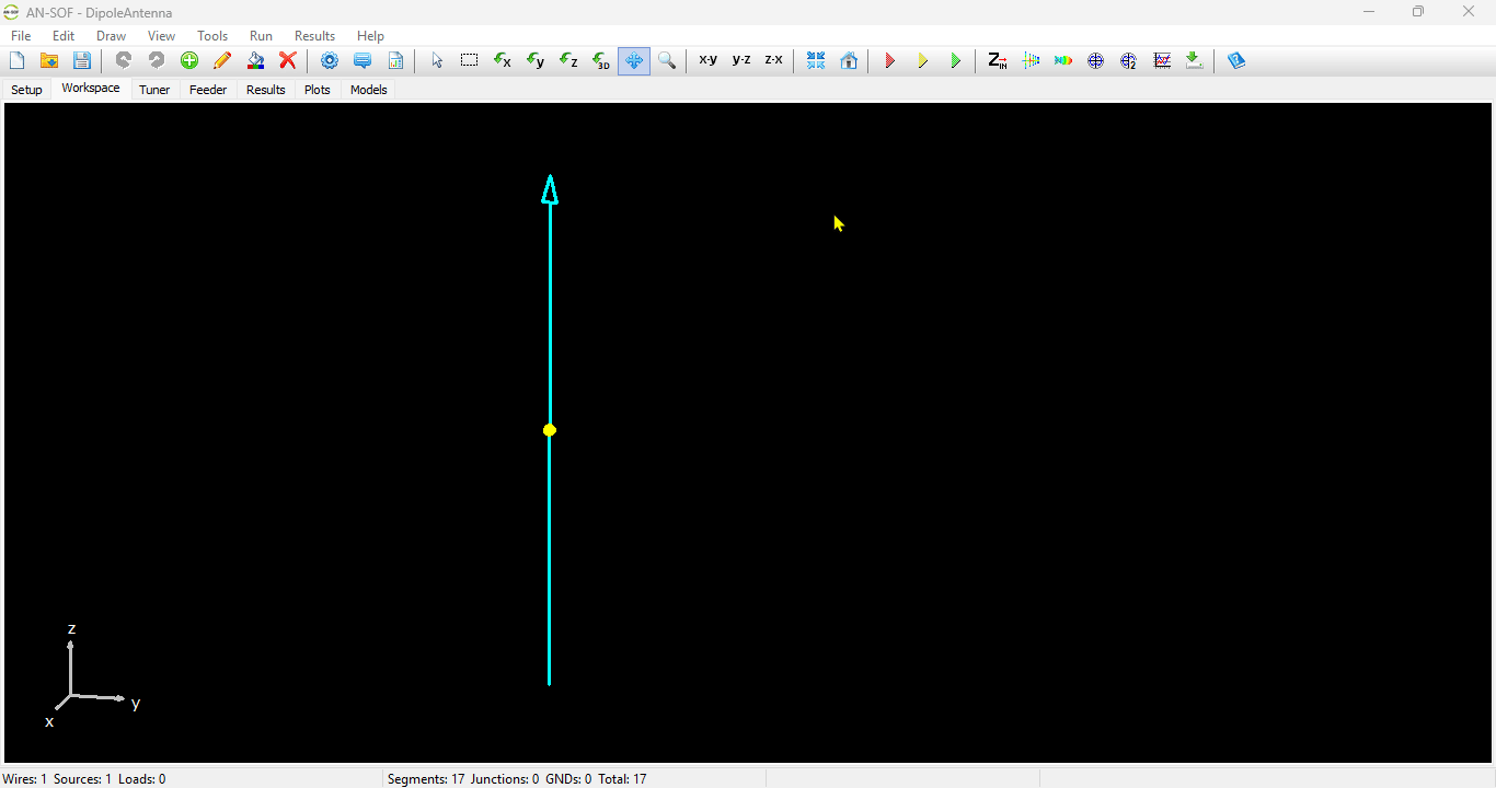
AN-SOF provides several ways to export your wire geometry and simulation settings for use in other software, ranging from legacy solvers to CAD tools and programming environments.
1. NEC Format (.nec)
Exporting to the Numerical Electromagnetics Code (NEC) format is ideal for benchmarking or using alternative solvers. To do this, navigate to File > Export Wires and select the .nec file type.
The software automatically translates your model into standard NEC “cards”:
- GW Lines: All linear wires are converted into geometry cards.
- Physics & Setup: The export includes cards for ground conditions (GN/GE), transmission lines (TL), loads and conductivity (LD), and insulation (IS).
- Simulation Parameters: Frequency (FR), excitation (EX), the “Exact Kernel” toggle (EK), and radiation pattern requests (RP) are also preserved.
2. CAD Exchange (DXF)
If you need to incorporate your antenna design into a mechanical drawing or a professional CAD environment (like AutoCAD or SolidWorks):
- Navigate to File > Export Wires and choose .dxf.
- Note: While the 3D paths and positions of the wires are maintained, the specific cross-section attributes (like the equivalent radius or shape) are lost in this format, as DXF treats the segments as basic lines.
3. Programming Scripts (.m / .sce)
For users who prefer automation and parametric modeling, you can export your project as a script for MATLAB/Octave (.m) or Scilab (.sce).
- Parametric Control: The exported file contains code that defines the wire lengths, positions, and frequencies.
- Customization: You can modify variables within the script to create loops, allowing you to sweep geometry parameters or generate complex, repeatable project configurations automatically.
Adding Wires
A Line represents a linear (straight) wire in AN-SOF.
Accessing the Line Dialog Box
To open the Line dialog box:
- Navigate to Draw > Line in the main menu.
- The dialog box contains three tabs: Line, Attributes, and Materials (Fig. 1).
Line Tab: Setting Geometrical Parameters
Two options are available for defining the line:
- 2 Points (Figs. 1 and 2)
- Define the line by specifying two points:
- From Point: Starting coordinates (X1, Y1, Z1).
- To Point: Ending coordinates (X2, Y2, Z2).
- Define the line by specifying two points:
- Start – Direction – Length (Figs. 3 and 4)
- Define the line by:
- Start Point: Initial coordinates (X1, Y1, Z1).
- Direction: Spherical angles (Theta, Phi).
- Wire Length: Total length of the line.
- Define the line by:
Attributes Tab
- Specify the Number of Segments and Cross-Section properties (refer to Wire Attributes).
Materials Tab
- Set the Resistivity and Coating properties of the wire (refer to Wire Materials).
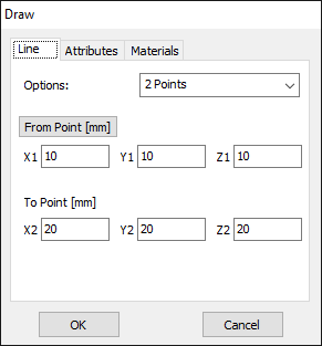
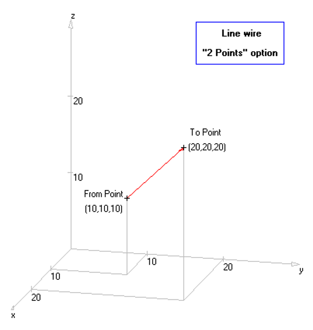
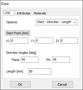
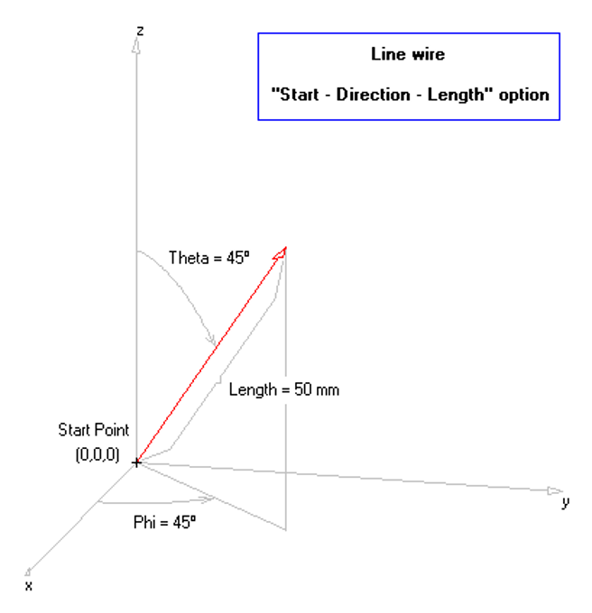
An Arc represents a circular arc in AN-SOF.
Accessing the Arc Dialog Box
To open the Arc dialog box:
- Navigate to Draw > Arc in the main menu.
- The dialog box contains three tabs: Arc, Attributes, and Materials (Fig. 1).
Arc Tab: Setting Geometrical Parameters
Two options are available for defining the arc:
- 3 Points (Figs. 1 and 2)
- Define the arc by specifying three points:
- Start Point: Starting coordinates (X1, Y1, Z1).
- Second Point: Second point coordinates (X2, Y2, Z2).
- End Point: Ending coordinates (X3, Y3, Z3).
- Define the arc by specifying three points:
- Start – Center – End (Figs. 3 and 4)
- Define the arc by:
- Start Point: Initial coordinates (X1, Y1, Z1).
- Center: Coordinates of the arc center (Cx, Cy, Cz).
- End Point: Ending coordinates (X2, Y2, Z2), which may not coincide with the actual ending point of the arc.
- Define the arc by:
Attributes Tab
- Specify the Number of Segments and Cross-Section properties (refer to Wire Attributes).
Materials Tab
- Set the Resistivity and Coating properties of the wire (refer to Wire Materials).
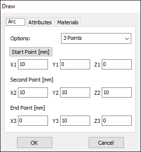
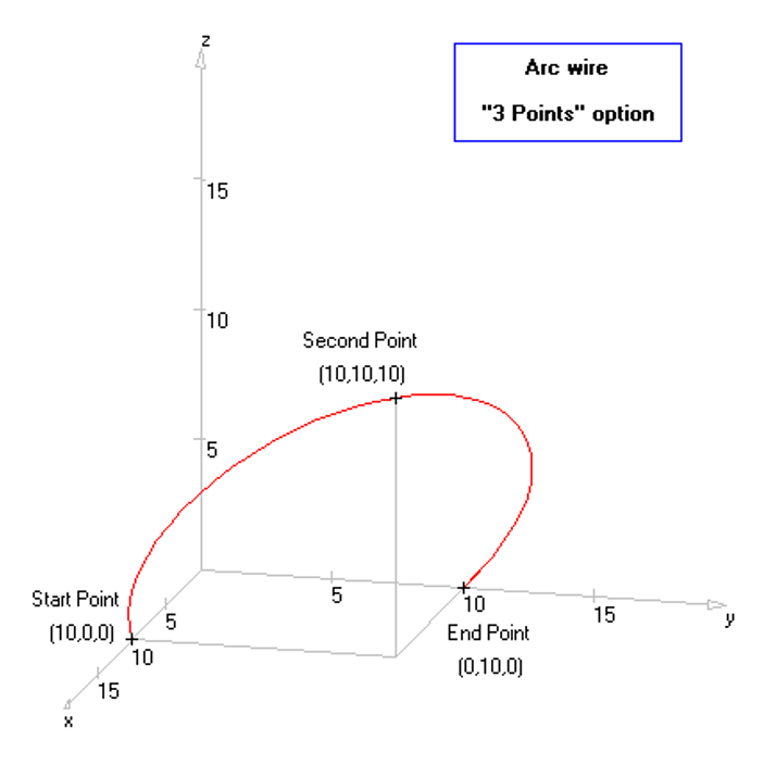
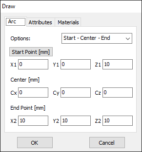
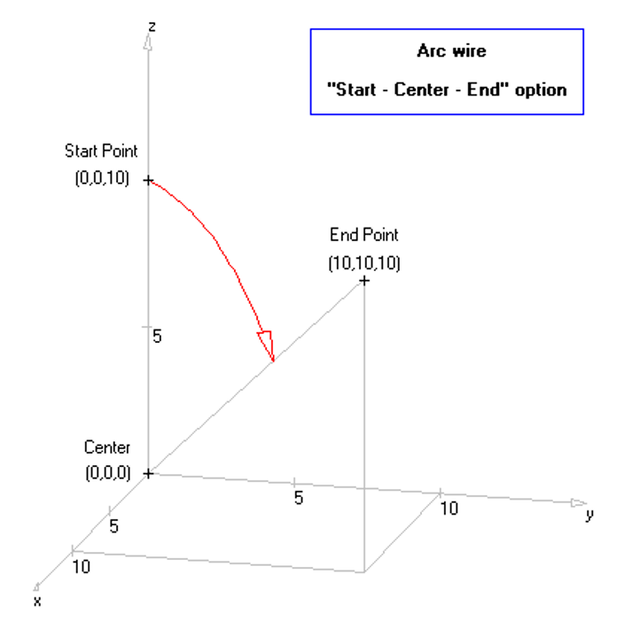
A Circle represents a circular loop in AN-SOF.
Accessing the Circle Dialog Box
To open the Circle dialog box:
- Navigate to Draw > Circle in the main menu.
- The dialog box contains four tabs: Circle, Orientation, Attributes, and Materials (Fig. 1).
Circle Tab: Setting Geometrical Parameters
Two options are available for defining the circle:
- Center – Radius – Orientation (Figs. 1, 2, and 3)
- Define the circle by specifying:
- Center: Coordinates of the circle center (Cx, Cy, Cz).
- Radius: Circle radius.
- Orientation Tab Enabled: Direction of the circle axis, set by the spherical angles (Theta, Phi) or a normal vector (Nx, Ny, Nz). The “rotation angle” rotates the circle around its axis.
- Define the circle by specifying:
- 3 Points (Figs. 4 and 5)
- Define the circle by:
- First Point: Initial coordinates (X1, Y1, Z1).
- Second Point: Second point coordinates (X2, Y2, Z2).
- Third Point: Third point coordinates (X3, Y3, Z3).
- Define the circle by:
Attributes Tab
- Specify the Number of Segments and Cross-Section properties (refer to Wire Attributes).
Materials Tab
- Set the Resistivity and Coating properties of the wire (refer to Wire Materials).
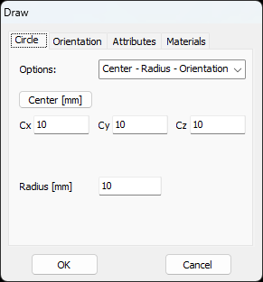
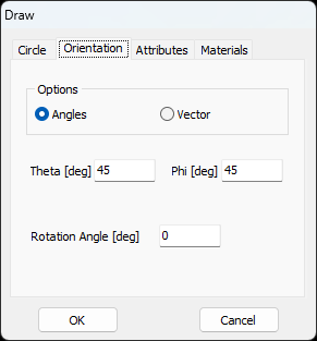
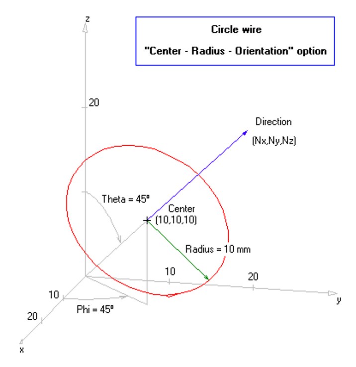
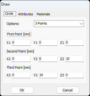
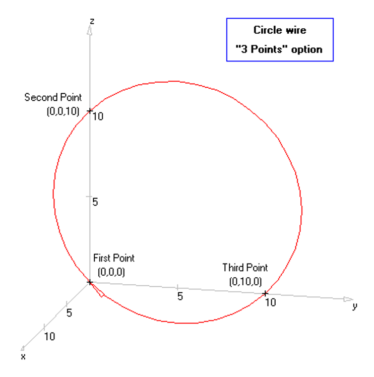
A Helix represents a circular helix in AN-SOF.
Accessing the Helix Dialog Box
To open the Helix dialog box:
- Navigate to Draw > Helix in the main menu.
- The dialog box contains four tabs: Helix, Orientation, Attributes, and Materials (Fig. 1).
Helix Tab: Setting Geometrical Parameters
Two options are available for defining the helix:
- Start – Radius – Pitch – Turns (Figs. 1, 2, and 3)
- Define the helix by specifying the following:
- Start Point: Starting coordinates (X1, Y1, Z1).
- Radius or Diameter: The helix radius or diameter; entering one will automatically calculate the other.
- Pitch (turn spacing) or Pitch Angle: The helix pitch or pitch angle; entering one will automatically calculate the other. A positive pitch results in a right-handed helix, while a negative pitch results in a left-handed helix.
- Nr. of Turns or Length: The number of turns or the filar length; entering one will automatically calculate the other. The number of turns does not need to be an integer, allowing for fractional turns.
- Height: The axial height from the starting point to the ending point. This value is calculated automatically and cannot be edited.
- Orientation Tab Enabled: Sets the direction of the helix axis using spherical angles (Theta, Phi) or a vector (Nx, Ny, Nz). The “rotation angle” rotates the helix around its axis.
- Define the helix by specifying the following:
- Start – End – Radius – Turns (Figs. 4 and 5)
- Define the helix by specifying the following:
- Start Point: Starting coordinates (X1, Y1, Z1).
- End Point: Ending coordinates (X2, Y2, Z2).
- Radius: The helix radius.
- Number of Turns: This must be an integer. A positive value results in a right-handed helix, while a negative value results in a left-handed helix.
- Rotation Angle: Rotates the helix around its axis.
- Height: The axial height from the starting point to the ending point. This value is calculated automatically and cannot be edited.
- Define the helix by specifying the following:
Attributes Tab
- Specify the Number of Segments and Cross-Section properties (refer to Wire Attributes).
Materials Tab
- Set the Resistivity and Coating properties of the wire (refer to Wire Materials).
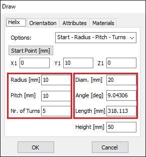
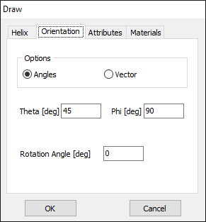
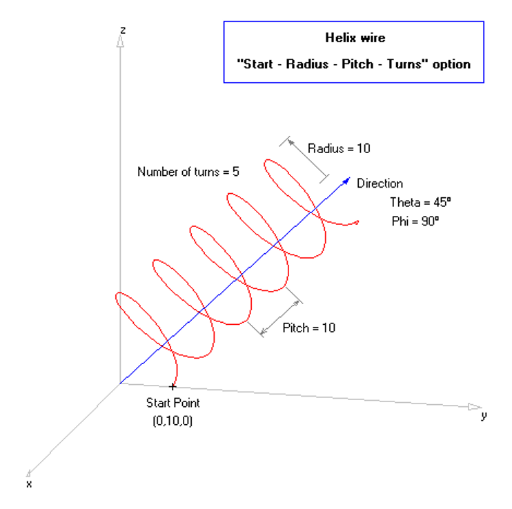
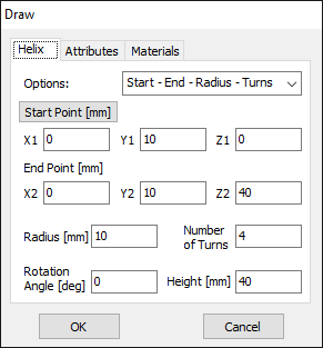
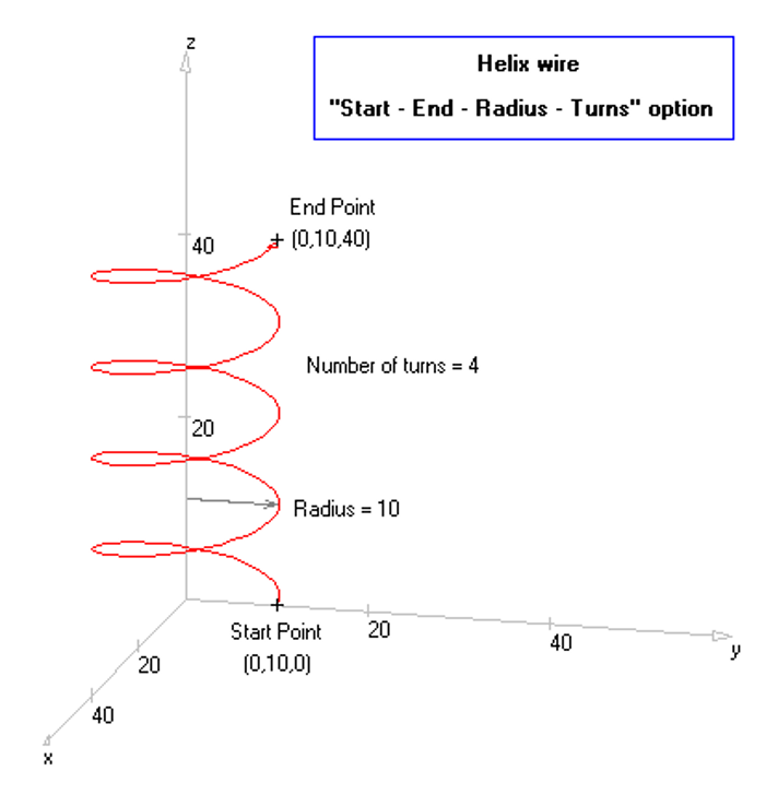
A Quadratic represents a parabola in AN-SOF.
Accessing the Quadratic Dialog Box
To open the Quadratic dialog box:
- Navigate to Draw > Quadratic in the main menu.
- The dialog box contains three tabs: Quadratic, Attributes, and Materials (Fig. 1).
Quadratic Tab: Setting Geometrical Parameters
Define the quadratic by specifying (Fig. 1):
- Start Point: Starting coordinates (X1, Y1, Z1).
- Second Point: Second point coordinates (X2, Y2, Z2).
- End Point: Ending coordinates (X3, Y3, Z3).
Attributes Tab
- Specify the Number of Segments and Cross-Section properties (refer to Wire Attributes).
Materials Tab
- Set the Resistivity and Coating properties of the wire (refer to Wire Materials).
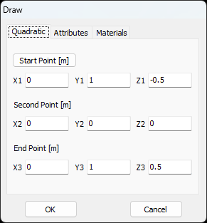
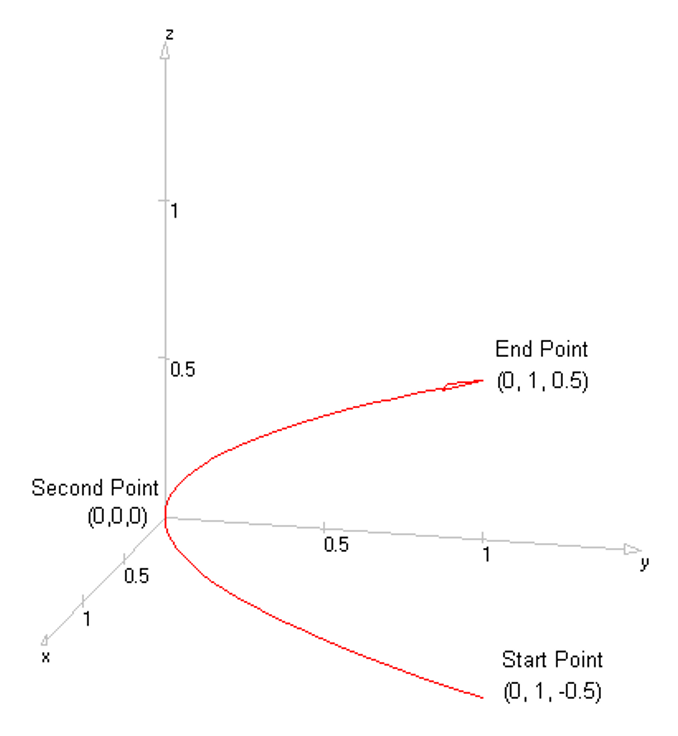
An Archimedean Spiral represents an Archimedes’ spiral in AN-SOF.
The Archimedean spiral is a planar spiral defined by the polar equation:
$\displaystyle r(\alpha) \,=\, r_0 \,+\, \frac{p}{2\pi} \; \alpha$
where $r_0$ is the starting radius, $p$ is the pitch, and $\alpha$ is the angle in the plane of the spiral, ranging from $0$ to $2\pi M$, with $M$ representing the number of turns.
The spiral’s starting radius is $r(0) = r_0$ and its ending radius is $r(2\pi M) = r_0 + pM$. Consequently, the pitch $p$ represents the constant spacing between consecutive turns. Additionally, the pitch is equal to the constant growth rate of the spiral radius $r(\alpha)$ per turn, expressed as:
$\displaystyle p \,=\, 2\pi \frac{dr}{d\alpha}$
Accessing the Archimedean Spiral Dialog Box
To open the Archimedean Spiral dialog box:
- Navigate to Draw > Archimedean Spiral in the main menu.
- The dialog box contains three tabs: Archimedean Spiral, Attributes, and Materials (Fig. 1).
Archimedean Spiral Tab: Setting Geometrical Parameters
Define the Archimedean spiral by specifying the following (Fig. 1):
- Start Point: Starting coordinates (X1, Y1, Z1).
- Start Radius: The initial radius of the spiral.
- Pitch: The constant spacing between turns (can be positive or negative).
- Number of Turns: This value does not need to be an integer, allowing for fractional turns.
- Orientation Angles: Sets the direction of the spiral axis using spherical angles (Theta, Phi).
- Rotation Angle: Rotates the spiral around its axis.
Attributes Tab
- Specify the Number of Segments and Cross-Section properties (refer to Wire Attributes).
Materials Tab
- Set the Resistivity and Coating properties of the wire (refer to Wire Materials).
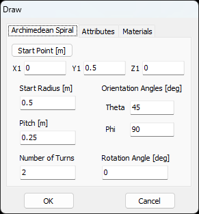
A Logarithmic Spiral represents an equiangular spiral in AN-SOF.
The logarithmic spiral (spira mirabilis) is defined by the polar equation:
$\displaystyle r(\alpha) \,=\, r_0 \, e^{b \alpha}$
where $r_0$ is the starting radius (the value of $r$ at $\alpha = 0$) and $b$ is a constant given by:
$\displaystyle b \,=\, \frac{p}{2\pi r_0}$
In this expression, $p$ represents the starting pitch, which is the derivative of the radius at the origin:
$\displaystyle p \,=\, 2\pi \, \frac{dr}{d\alpha} \bigg|_{\alpha \,=\, 0}$
This value $p$ corresponds to the initial growth rate of the spiral radius $r(\alpha)$ per turn. The angle $\alpha$ ranges from $0$ to $2\pi M$, where $M$ is the number of turns.
The first three terms of the Taylor expansion of the radius around $\alpha = 0$ are:
$\displaystyle r(\alpha) \,=\, r_0 \,+\, \frac{p}{2\pi} \alpha \,+\, \frac{r_0 (b \alpha)^2}{2} \,+\, \dots$
The linear portion of this expansion ($r_0 + p/(2\pi) \, \alpha$) provides the polar equation of an Archimedean spiral.
Accessing the Logarithmic Spiral Dialog Box
To open the Logarithmic Spiral dialog box:
- Navigate to Draw > Logarithmic Spiral in the main menu.
- The dialog box contains three tabs: Logarithmic Spiral, Attributes, and Materials (Fig. 1).
Logarithmic Spiral Tab: Setting Geometrical Parameters
Define the logarithmic spiral by specifying the following (Fig. 1):
- Start Point: Starting coordinates (X1, Y1, Z1).
- Start Radius: The initial radius of the spiral at the starting point.
- Start Pitch: The initial pitch (turn spacing) of the spiral; this value can be positive or negative.
- Number of Turns: The total number of turns; this does not need to be an integer, allowing for fractional turns.
- Orientation Angles: Sets the direction of the spiral axis using spherical angles (Theta, Phi).
- Rotation Angle: Rotates the spiral around its axis.
Attributes Tab
- Specify the Number of Segments and Cross-Section properties (refer to Wire Attributes).
Materials Tab
- Set the Resistivity and Coating properties of the wire (refer to Wire Materials).
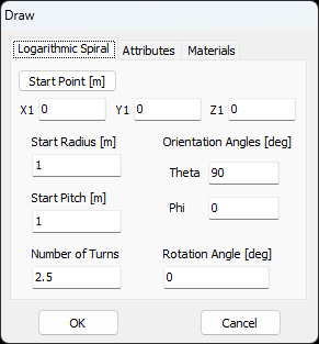
A tapered wire is a wire whose radius varies along its length. Because the change in radius occurs in discrete increments, it is also known as a stepped-radius wire. Tapered wires always have a circular cross section, and the radius typically changes linearly in defined steps—resulting in a wire with sections of constant radius, as illustrated in Fig. 1.
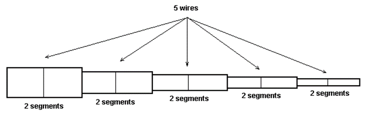
To draw a tapered wire, go to Draw > Tapered Wire in the main menu and select a wire type. The available types (e.g., Line, Arc, Circle) are the same as those found under the Draw menu. For example, Fig. 2 shows the Line page of the Draw dialog box when a linear wire type is selected.
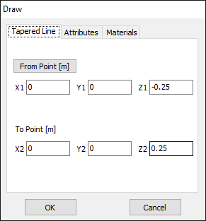
The wire must be divided into wire portions based on the desired number of radius steps, as indicated in Fig. 1. Each wire portion with a constant radius should then be subdivided into segments as required by the Method of Moments used in the simulation.
You can define the number of wire portions and the number of segments per portion in the Attributes tab (see Fig. 3). Here, you can also specify the start and end radii of the taper. To set the material properties—including the resistivity of the wire and any coating—use the Materials tab (see Fig. 4). A tapered coating can be specified by assigning start and end thickness values.
In the workspace, wire portions are shown in alternating colors for easier identification.
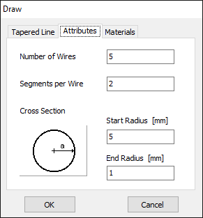
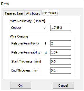
Supported Formats
To import wires from an external file into AN-SOF, follow these steps:
- Navigate to File > Import Wires in the main menu.
- A sub-menu with three options will be displayed: AN-SOF, NEC, and MM formats.
- Note that the MM format should contain only linear wires in ASCII text format.
AN-SOF Format
Wires can be imported into the AN-SOF workspace from another AN-SOF project. When a project is saved, a corresponding file with a .wre extension is created in the same directory. This file, named after the project, contains the geometrical description of all wires within the project. For details on files generated during project saves, refer to File Formats.
To import wires into your project, navigate to the main menu and select File > Import Wires > AN-SOF Format. Then, choose the specific .wre file you wish to import. You can import multiple .wre files, one at a time, as needed.
NEC Format
There are slight differences between the commands supported by AN-SOF and the standard NEC cards. To maintain compatibility with the NEC format, originally designed for data entry using punch cards, some fields appear repeating, and others must be entered with a zero, having no meaning. Lengths and wire radii are assumed to be in meters. If errors are found while importing a file, an error report will be shown in the Note panel of the Setup tab.
The SY command for symbolic variables is not supported. To run simulations with variable geometric parameters, you can write a script to sweep those parameters and generate the corresponding NEC files, then use the Run Bulk Simulation feature (see Running a Bulk Simulation).
For optimization tasks, you’ll need an optimizer script and should work with the AN-SOF Engine. Examples of parameter sweeps and optimization scripts are available in the Scripts & Optimizers category.
GW – Linear Wire
One linear wire per line must be set, beginning with “GW” and ending with an Enter, as follows:
GW Tag Segments X1 Y1 Z1 X2 Y2 Z2 Radius
[Enter]
Tag: Tag number for the linear wire (Tag > 0). The space between “GW” and Tag is optional. A single tab or comma can also be used as a separator between the command name and the first data field.
Segments: Number of segments for the wire. If zero is entered, the minimum recommended number of segments will be computed.
X1 Y1 Z1: Cartesian coordinates of the start point of the linear wire.
X2 Y2 Z2: Cartesian coordinates of the end point of the linear wire.
Radius: Wire radius.
Fields can be separated by up to two spaces, a single tab, a single comma, or a comma and space. Each GW line, including the last one in a set of linear wires to be imported, must end with an Enter (press Enter on the keyboard for a carriage return). The text lines above the GW lines will be ignored, so comments can be added at the beginning of the file.
The following are equivalent examples:
Write comments here
GW 1 12 5.42 0.38 1.262 5.425 -0.378 1.261 0.01[Enter]
GW 2 5 7.45 0 1.122 7.45 0 1.49 0.015[Enter]
GW 3 2 8.3 0.0 1.12 8.37 0.0 1.595 0.01[Enter]
Write comments here
GW1,12,5.42,0.38,1.262,5.425,-0.378,1.261,0.01[Enter]
GW2,5,7.45,0,1.122,7.45,0,1.49,0.015[Enter]
GW3,2,8.3,0.0,1.12,8.37,0.0,1.595,0.01[Enter]
CM and Other Commands
The following commands: CM (comment lines), GH (helical wire), GA (arc), GM (coordinate transformation), GS (scale dimensions), GE (ground connections), GN (real ground parameters), TL (transmission line), LD (load impedances and wire conductivity), IS (insulated wire), FR (frequency), EX (excitation), EK (exact kernel), and RP (radiation pattern), will also be read.
CM lines will be added to the Note panel of the Setup tabsheet after the NEC file is imported. The comment termination card, “CE”, is not needed in AN-SOF. Comments without the CM command at the beginning of the file will be ignored and not imported. The command names—“CM”, “GW”, “GH”, etc.—are reserved words in AN-SOF and are used to recognize the fields between these commands and the final Enter in each text line, so the command names should not be used in comments.
IMPORTANT: CM lines must always be placed at the beginning of a .nec file and kept separate from other commands.
The rest of the AN-SOF commands in NEC format are listed below, where all the indicated fields are mandatory.
GH – Helix
The GH command is used to define a helix in AN-SOF with the following syntax:
GH Tag Segments Spacing Length R R R R Radius
[Enter]
Tag: A positive number representing the tag for the helix. The space between “GH” and the Tag is optional. Note that the helix begins at the origin and develops along the positive z-axis. To adjust the helix’s position or rotation, use the GM command described below. It’s important to mention that the GH command differs in NEC-4.
Segments: The number of segments for the helix. If zero is entered, AN-SOF will compute the minimum recommended number of segments. Unlike NEC, AN-SOF uses conformal segments that precisely follow the helix contour.
Spacing: Spacing between turns.
Length: Total length of the helix. A positive Length value results in a right-handed helix, while a negative Length value produces a left-handed helix.
R: Radius of the helix (repeated four times).
Radius: Wire radius.
Note: AN-SOF uses conformal segments that exactly follow the helix contour, distinguishing it from NEC.
GA – Arc
The GA command is utilized to define an arc in AN-SOF with the following syntax:
GA Tag Segments R Ang1 Ang2 Radius
[Enter]
Tag: A positive number serving as the tag for the arc. The space between “GA” and the Tag is optional. The arc is situated on the xz-plane, centered at the origin, making the y-axis the axis of the arc. To manipulate the position or rotation of the arc, use the GM command described below.
Segments: The number of segments for the arc. If zero is entered, AN-SOF will compute the minimum recommended number of segments. It’s worth noting that, unlike NEC, AN-SOF uses conformal segments that precisely follow the arc contour.
R: Arc radius.
Ang1: The angle of the first end of the arc measured from the x-axis in a left-handed direction about the y-axis, given in degrees.
Ang2: The angle of the second end of the arc, measured in degrees.
Radius: Wire radius.
Note: AN-SOF uses conformal segments that exactly follow the arc contour, distinguishing it from NEC.
GB – AN-SOF’s Arc
The GB command is utilized to define an arc in AN-SOF with the following syntax:
GB Tag Segments Type X1 Y1 Z1 X2 Y2 Z2 X3 Y3 Z3 Radius
[Enter]
Tag: A positive number serving as the tag for the arc. The space between “GB” and the Tag is optional.
Segments: The number of segments for the arc. If zero is entered, AN-SOF will compute the minimum recommended number of segments. It’s worth noting that, unlike NEC, AN-SOF uses conformal segments that precisely follow the arc contour.
Type: Type of arc. Set Type = 0 for entering three points, and Type = 1 for entering the start point, center, and end point.
X1 Y1 Z1: Cartesian coordinates of the start point of the arc.
X2 Y2 Z2: Cartesian coordinates of the second point of the arc if Type = 0, or the arc center if Type = 1.
X3 Y3 Z3: Cartesian coordinates of the end point of the arc.
Radius: Wire radius.
Note: AN-SOF uses conformal segments that exactly follow the arc contour, distinguishing it from NEC. The “GB” command is exclusive to AN-SOF and cannot be found in any NEC version.
GM – Coordinate Transformation
The GM command in AN-SOF facilitates coordinate transformations with the following syntax:
GM 0 N rotX rotY rotZ DX DY DZ 0
[Enter]
N: If N is set to 0, it implies that the entire structure above the GM command must undergo rotation and translation based on the specified values for (rotX, rotY, rotZ) and (DX, DY, DZ). The coordinate transformations are applied sequentially in that order. If N is set to 1, it indicates that the structure above the GM command must be copied, and the copy should be moved to a new position (DX, DY, DZ) from the origin. You can use the “GM” command below the “GW,” “GH,” and “GA” commands to rotate, move, and copy linear wires, helices, and arcs as needed.
rotX: Angle of rotation about the X-axis, specified in degrees.
rotY: Angle of rotation about the Y-axis, specified in degrees.
rotZ: Angle of rotation about the Z-axis, specified in degrees.
DX: Translation along the X-axis, moving the structure by an amount DX.
DY: Translation along the Y-axis, moving the structure by an amount DY.
DZ: Translation along the Z-axis, moving the structure by an amount DZ.
GS – Scale Structure Dimensions
The GS command in AN-SOF is used for scaling structure dimensions. The syntax is as follows:
GS 0 0 Scale
[Enter]
Scale: This represents the scaling factor. Applying this command results in the multiplication of all structure dimensions, including wire radii, by the specified scale value.
GE – Ground Connections
The GE command in AN-SOF is used for defining ground connections. The syntax is as follows:
GE Type
[Enter]
Type = 0: No ground plane is present. If a “GE” command is used without specifying a type, it will be interpreted as “GE 0”.
Type = 1: A PEC ground plane is placed at z = 0, and wires ending on the ground plane will be connected to the ground. If a real ground plane has been chosen, Type = 1 indicates that the wire connections to the ground must be considered as zero-Ohm connections.
Type = -1: The wire connections to the ground are imperfect and produce power losses when a real ground plane has been chosen.
GN – Real Ground
The GN command in AN-SOF is used for defining real ground parameters. The syntax is as follows:
GN Type Screen 0 0 Epsilon Sigma Length WireRadius
[Enter]
Type: Type of ground plane.
- Type = -1: Free space simulation; all ground parameters are ignored. “GN -1” can be used in this case.
- Type = 0: Reflection Coefficients/Asymptotic option.
- Type = 1: PEC ground plane at z = 0; other parameters are ignored. “GN 1” can be used in this case.
- Type = 2: Sommerfeld-Wait/Asymptotic option.
Screen: Number of radials in a radial wire ground screen. Set Screen = 0 if no ground screen is present.
Epsilon: Ground plane relative permittivity or dielectric constant.
Sigma: Ground plane conductivity in [S/m].
Length: Length of radial wires if a radial wire ground screen is used. Enter zero if no ground screen is used.
WireRadius: Radius of radial wires if a screen is used. Enter zero if no ground screen is used.
TL – Transmission Line
The TL command in AN-SOF is used to define a transmission line. The syntax is as follows:
TL Tag1 Seg1 Tag2 Seg2 Zc Length Y1r Y1i Y2r Y2i
[Enter]
Tag1: Wire tag number to which the first port of the transmission line connects.
Seg1: Segment number of wire Tag1 to which the first port of the transmission line connects.
Tag2: Wire tag number to which the second port of the transmission line connects.
Seg2: Segment number of wire Tag2 to which the second port of the transmission line connects.
Zc: Characteristic impedance of the transmission line in Ohms. A negative Zc can be entered to set a “crossed” transmission line with a 180° phase reversal relative to the reference directions of the segments. The characteristic impedance of the line is |Zc|.
Length: Length of the transmission line in meters. If Length = 0, the linear distance between the transmission line ports will be considered as the length for the line. To simulate a zero-length transmission line, enter 1E-10.
Y1r: Real part of the shunt admittance across end one of the transmission line [S].
Y1i: Imaginary part of the shunt admittance across end one of the transmission line [S].
Y2r: Real part of the shunt admittance across end two of the transmission line [S].
Y2i: Imaginary part of the shunt admittance across end two of the transmission line [S].
Refer to Adding Transmission Lines for a review of considerations when setting transmission lines, including advanced settings not available with the TL command.
LD – Load Impedance
The LD command in AN-SOF is used to define a load impedance. The syntax is as follows:
LD Type Wire# Seg# Seg# R L C
[Enter]
Type: Type of load. Series/parallel/trap RLC loads, fixed impedances R+jX, and wire conductivity can be set.
- Set Type = 0 for a series RLC load.
- Set Type = 1 for a parallel RLC load.
- Set Type = 4 for a fixed impedance R+jX. The reactance “X” must be entered in the position of “L” (the “C” field will be ignored). The reactance is fixed, so it does not scale with frequency.
- Set Type = 5 and Seg# = 0 to specify a wire conductivity [S/m] in the “R” field for the wire number “Wire#”. Use the command LD 5 0 0 0 R 0 0 to set a conductivity “R [S/m]” on all wires. “LD 5” command for setting wire conductivity must be below all LD 0, LD 1, LD 4, and LD 6 lines.
- Set Type = 6 for a trap RLC load (series RL + parallel C).
Wire#: Wire tag number where the load or conductivity is placed.
Seg#: Segment number where the load is placed. Note that it appears twice due to a NEC convention not used in AN-SOF, so the second Seg# will be ignored. Set Seg# = 0 if a wire conductivity is to be entered.
R: Resistance in Ohms or conductivity in S/m.
L: Inductance in Henries when Type = 0, or reactance in Ohms when Type = 4 (it does not scale with frequency). The “L” field is ignored if R is a conductivity, so a zero can be entered.
C: Capacitance in Farads; if none, enter zero. It is ignored if R is a conductivity, so enter zero.
IS – Insulated Wire
The IS command in AN-SOF is used to define an insulated wire. The syntax is as follows:
IS 0 Wire# 0 0 Epsilon 0 Radius
[Enter]
Wire#: Wire tag number where the insulation or coating will be applied.
Epsilon: Relative permittivity of the dielectric sheath.
Radius: Radius of the insulating sheath. Ensure it is greater than the wire radius.
FR – Frequencies
The FR command in AN-SOF defines the frequencies used in a simulation. Its syntax is:
FR Type Num 0 0 Freq Df
[Enter]
Type: Specifies the type of frequency sweep. For a linear sweep, set Type = 0; for a logarithmic sweep, set Type = 1.
Num: Number of frequency steps (Num ≥ 1).
Freq: Frequency in MHz, or the starting frequency for a range.
Df: If Type = 0, it represents the frequency stepping increment in MHz. If Type = 1, it is the multiplication factor for a logarithmic sweep.
To simulate at a single frequency, use: FR 0 1 0 0 Freq 0
EX – Excitation
The EX command in AN-SOF is used to define excitation sources for simulations. The syntax is as follows:
EX Type Wire# Seg# 0 Real Imag
[Enter]
Type: Type of source. Use Type = 0 or 5 (the “5” corresponds to an old source model used in NEC) for a voltage source. Set Type = 6 for a current source. Note that current sources in AN-SOF automatically have a non-zero internal impedance set in parallel with the source (1E6 Ohm).
Wire#: Wire tag number where the source is placed.
Seg#: Segment where the source is located.
Real: Real part of the source voltage or current.
Imag: Imaginary part of the source voltage or current.
EK – Exact Kernel
The EK command in AN-SOF is used to force the use of the Exact Kernel. The syntax is as follows:
EK
[Enter]
This command ensures that the Exact Kernel is utilized, even if this option is disabled. It’s important to note that AN-SOF has the Exact Kernel enabled by default.
RP – Radiation Pattern
The RP command in AN-SOF is used to set the radiation pattern parameters. The syntax is as follows:
RP 0 Ntheta Nphi 1001 Theta Phi Dtheta Dphi R
[Enter]
Ntheta: Number of values of Θ at which the field is to be computed.
Nphi: Number of values of φ at which the field is to be computed.
(Note: The value “1001” is a NEC variable and will be ignored since AN-SOF always computes the average power gain.)
Theta: Initial Θ angle in degrees.
Phi: Initial φ angle in degrees.
Dtheta: Increment for Θ in degrees.
Dphi: Increment for φ in degrees.
R: Radial distance in meters of the field point from the origin. R = 0 is taken as R = 1 m.
MM Format
One linear wire per line must be defined as follows:
X1,[TAB]Y1,[TAB]Z1,[TAB]X2,[TAB]Y2,[TAB]Z2,[TAB]Radius,[TAB]Segments
[Enter]
X1 Y1 Z1 = Cartesian coordinates of the wire start point.
X2 Y2 Z2 = Cartesian coordinates of the wire end point.
Radius = Wire radius.
Segments = Number of segments.
The last text line must end with an Enter (press Enter in the keyboard for a carriage return).
Example:
5.42, 0.38, 1.262, 5.425, -0.378, 1.261, 0.01, 12
7.45, 0, 1.122, 7.45, 0, 1.49, 0.015, 5
8.3, 0.0, 1.12, 8.37, 0.0, 1.595, 0.01, 2
[Enter]
In the MM format, a wire can be automatically segmented by specifying any number less than or equal to zero for the segment count. The coordinates of each wire’s start and end points must use the same length unit selected in the Preferences dialog box in AN-SOF. Similarly, the radius of any imported wire must also be expressed in the selected unit.
Linear wires can be entered and edited in a table using the Tabular Input window. To access this feature, navigate to Draw > Tabular Input (Ctrl + T) in the main menu. This opens the Tabular Input window (see Fig. 1), which contains four tabs:
- Wires:
- Allows you to enter and edit linear wires by specifying their end coordinates, number of segments, wire radius, and materials.
- Sources:
- Enables you to connect sources to the wires listed in the Wires tab. A source must be connected to a specific wire segment.
- Loads:
- Allows you to connect loads to the wires listed in the Wires tab. A load must be connected to a specific wire segment.
- Trans. Lines:
- Enables you to connect transmission lines between two wire segments listed in the Wires tab.
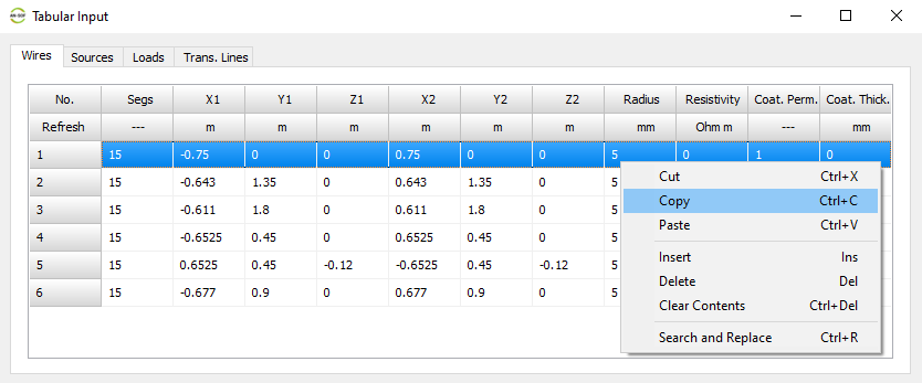
Wires Tab
Select the Wires tab and enter values as specified in the column titles (see Fig. 1). Each row corresponds to a linear wire, and you can input details such as:
- Number of segments (Segs).
- Coordinates of the starting point (X1, Y1, Z1) and ending point (X2, Y2, Z2).
- Wire radius.
- Resistivity.
- Coating (dielectric insulation).
Note: Only wires with a circular cross-section can be entered.
Table Interaction
- Right-click on the table to open a pop-up menu with standard options such as Cut (Ctrl + X), Copy (Ctrl + C), and Paste (Ctrl + V).
- Single cells can be selected by left-clicking on them or by using the TAB and arrow keys on the keyboard.
- Rows can be selected by clicking on the row number in the left column (No. column). Use the mouse or the up/down arrow keys to select a single row. The selected wire (row) is highlighted in red in the workspace. Double-click on a cell to exit row selection mode.
Row Operations
- Use Cut (Ctrl + X), Copy (Ctrl + C), and Paste (Ctrl + V) to manipulate selected rows.
- Use the Insert (Ins key) and Delete (Del key) options to add or remove rows.
- The Clear Contents (Ctrl + Del) option clears the content of a selected cell or row.
- The Search and Replace (Ctrl + R) option allows for bulk edits to wire end coordinates.
Wire Numbers in the Workspace
While the Tabular Input window is open, wire numbers are displayed in the workspace next to the corresponding wires (see Fig. 2). These numbers indicate the order of the wires in the table.
Note:
- Wires do not have permanent tags in AN-SOF. If a wire is deleted, the numbers will adjust automatically.
- Wire numbers are used solely for identification in the workspace while the Tabular Input window is open.
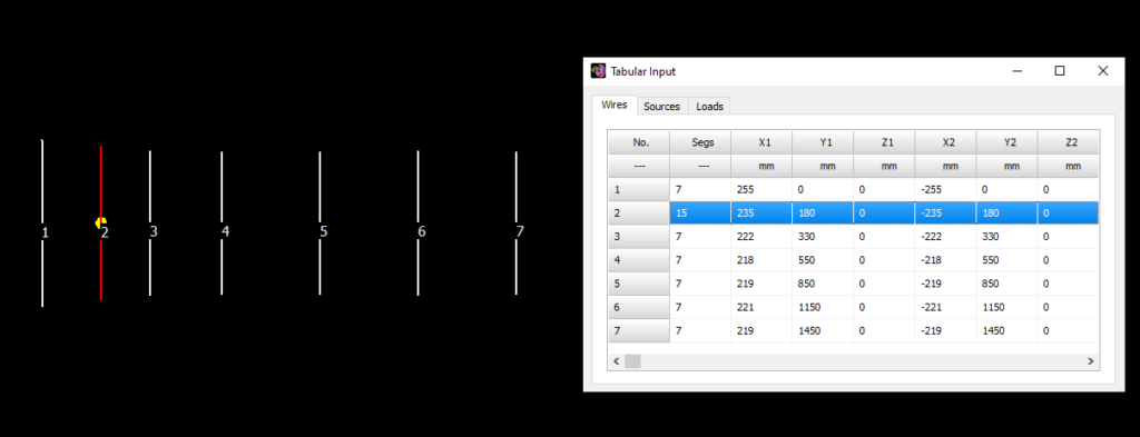
Sources Tab
Use the Sources tab to enter sources (see Fig. 3).
Entering Source Details
- Type Column: Enter “V” for a voltage source or “I” for a current source.
- Wire No. Column: Specify the wire on which the source is placed. Refer to the wire numbering in the No. column of the Wires tab.
- Position Column: Indicate the segment number where the source is connected. The segment number ranges from 1 to the number of segments (Segs) specified for the wire in the Wires tab.
- Amplitude Column: Enter the amplitude of the source in Volts or Amperes.
- Phase Column: Specify the phase of the source in degrees.
Table Interaction
- Right-click on the table to open a pop-up menu with standard options:
- Cut (Ctrl + X)
- Copy (Ctrl + C)
- Paste (Ctrl + V)
- Insert (Ins key)
- Delete (Del key)
- Clear Contents (Ctrl + Del)
These options function the same way as in the Wires tab, allowing you to manipulate cells and rows.
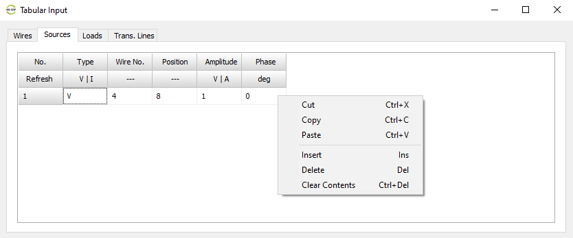
Loads Tab
Use the Loads tab to enter load impedances (see Fig. 4).
Entering Load Details
- Type Column: Enter one of the following:
- “L” for an inductor.
- “C” for a capacitor.
- “Z” for an impedance (R + jX).
- Wire No. Column: Specify the wire on which the load is placed. Refer to the wire numbering in the No. column of the Wires tab.
- Position Column: Indicate the segment number where the load is connected. The segment number ranges from 1 to the number of segments (Segs) specified for the wire in the Wires tab.
- R Column: Enter the resistance value (R) in Ohms.
- Last Column: Depending on the option entered in the Type column, input one of the following:
- Inductance (L) in the displayed unit.
- Capacitance (C) in the displayed unit.
- Reactance (X) in Ohms.
Table Interaction
- Right-click on the table to open a pop-up menu with standard options:
- Cut (Ctrl + X)
- Copy (Ctrl + C)
- Paste (Ctrl + V)
- Insert (Ins key)
- Delete (Del key)
- Clear Contents (Ctrl + Del)
These options function the same way as in the Wires tab, allowing you to manipulate cells and rows.
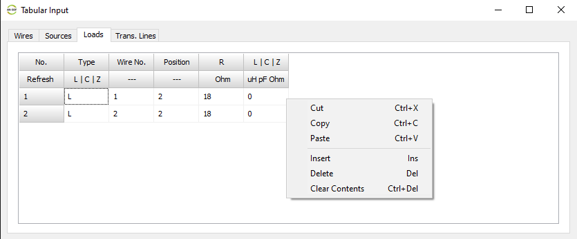
Trans. Lines Tab
Use the Trans. Lines tab to enter transmission lines and connect them to wire segments (see Fig. 5).
Entering Transmission Line Details
- Port 1 Columns:
- Specify the wire segment where Port 1 of the transmission line is connected by entering the Wire No. and Position. Refer to the numbering and number of segments specified for each wire in the Wires tab.
- Port 2 Columns:
- Similarly, specify the wire segment where Port 2 of the transmission line is connected by entering the Wire No. and Position.
- Additional Columns:
- Complete the Type, Z0 (characteristic impedance), VF (velocity factor), Length, and other columns as explained in the section Adding Transmission Lines.
- To simplify the process, select a row and double-click on an option in the right panel, which contains a collection of transmission line types with preloaded parameters.
Table Interaction
- Right-click on the table to open a pop-up menu with standard options:
- Cut (Ctrl + X)
- Copy (Ctrl + C)
- Paste (Ctrl + V)
- Insert (Ins key)
- Delete (Del key)
- Clear Contents (Ctrl + Del)
These options function the same way as in the Wires tab, allowing you to manipulate cells and rows.
Note:
- Entering a zero in Wire No., regardless of the Position entered, disconnects the port from the wire (putting the transmission line port in FREE status).
- Only transmission lines with both ports connected to wire segments will be considered in a simulation.
- Clicking on a row number (first column of the table) in the Trans. Lines tab highlights the transmission line in red in the AN-SOF workspace.
Refresh Button
A Refresh button is located just below the No. cell in all tabs of the Tabular Input window (see Fig. 6). Click the Refresh button to instantly apply changes. This eliminates the need to close and reopen the Tabular Input window to apply modifications.
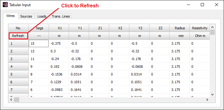
Editing Wires
Ways to Select a Wire
Selecting a wire in the workspace allows you to edit it, visualize its properties, or view simulation results. You can select any wire using one of the following methods:
- Using the Select Wire Tool: Click the Select Wire button (arrow icon) on the toolbar, and then left-click on the desired wire.
- Right-Clicking the Wire: Right-click on the wire to open a pop-up menu (see Fig. 1).
- Using Keyboard Shortcuts: Press F8 or F9 to select wires one by one, either forwards or backwards, in the order they were created.
Double-click on the workspace or press ESC to deselect the wire.
When a wire is selected, it will be highlighted in light blue for easy identification. Once selected, you can:
- Edit the wire.
- View its properties, such as geometrical details, electrical length, number of segments, wire radius, and materials.
- Visualize simulation results, such as current distribution or input impedance (if the wire has a source on one of its segments).
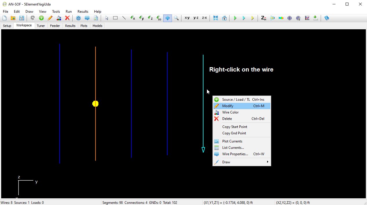
The Pop-Up Menu
Right-clicking on a wire opens a pop-up menu with the following commands:
Source / Load / TL (Ctrl + Ins)
Opens the Source / Load / TL toolbar, allowing you to connect a source, load impedance, or transmission line to a segment of the selected wire.
Modify (Ctrl + M)
Opens the Modify dialog box to edit the selected wire.
Wire Color
Opens a dialog box to change the color of the selected wire.
Delete (Ctrl + Del)
Deletes the selected wire, including all sources and loads placed on it. Transmission line connections will also be removed.
Copy Start Point
Copies the start point of the selected wire, enabling you to connect it to the end of another wire.
Copy End Point
Copies the end point of the selected wire, enabling you to connect it to the end of another wire.
Plot Currents
Opens a chart in the AN-XY Chart application, displaying the current distribution along the selected wire. This option is enabled only after currents have been computed.
List Currents
Opens the List Currents toolbar, allowing you to select a wire segment and tabulate its current versus frequency. This option is enabled only after currents have been computed.
Wire Properties (Ctrl + W)
Opens the Wire Properties dialog box, where you can view the geometry, attributes, and material data of the selected wire.
Draw
Contains a sub-menu with commands to draw various types of wires, including:
To modify an existing wire, right-click on it and choose Modify from the pop-up menu. This opens the Modify dialog box, where you can adjust the wire’s geometric parameters, attributes, and materials.
Alternatively, you can use the Select Wire button (arrow icon) from the main toolbar. After clicking this button, left-click on the wire you wish to modify. Once selected, go to Edit > Modify in the main menu. Note that this option is only enabled when a wire is selected.
Figure 1 shows how to access the Modify command for a linear wire.
To delete a wire, right-click on it and select Delete from the pop-up menu. This will remove the selected wire from the model. Note that any sources or loads attached to the wire will also be deleted.
Alternatively, you can delete a wire using the Select Wire button (arrow icon) in the main toolbar. Click the button, then left-click on the wire to select it. Once selected, go to Edit > Delete in the main menu. This option is only enabled when a wire is selected.
Figure 1 shows how to delete a linear wire using these options.
To enable a confirmation prompt before deleting a wire, go to Tools > Preferences > Options and check the option “Ask before deleting wires.”
AN-SOF allows you to simultaneously edit a group of wires. There are three ways to select multiple wires for editing:
- Using the Box Select Tool: Drag a rectangular box to select multiple wires.
- Using the Pick Tool: Left-click on individual wires while holding the Ctrl key.
- Combination of Both Methods: Use a mix of the Box Select tool and wire-by-wire selection.
Using the Box Select Tool
- Click the Box Select button on the main toolbar.
- Left-click on the workspace and drag a box to select multiple wires (see Fig. 1).
- All wires within the selection box will be highlighted in light blue.
- Dragging the box from top to bottom selects only fully enclosed wires.
- Dragging the box from bottom to top selects partially enclosed wires as well.
- Enclosing already selected wires with the selection box will deselect them.
- To deselect all wires, double-click on the screen or press ESC.
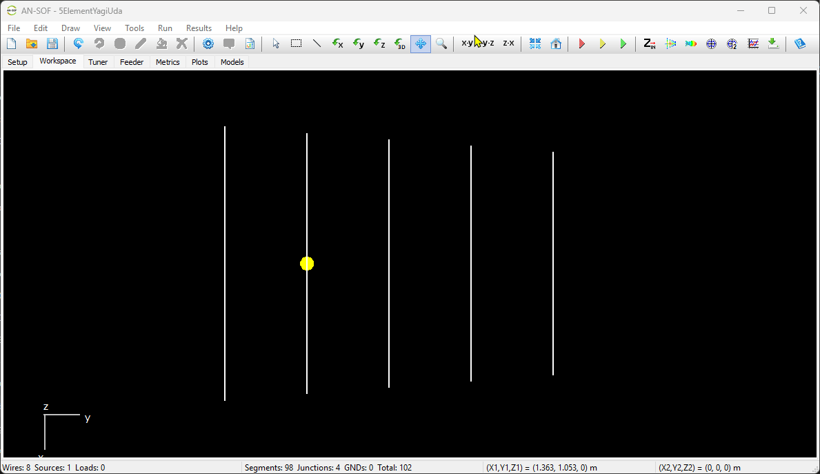
Selecting Wire by Wire
- Click the Pick Tool button (arrow icon) on the main toolbar (Fig. 2).
- Hold the Ctrl key and left-click on individual wires to select them.
- To deselect a wire, hold the Ctrl key and click on it again.
- To deselect all wires, double-click on the screen or press ESC.
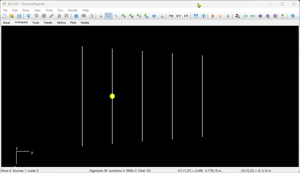
Wire Selection Methods – Video Tutorial
Watch the video below to learn how to efficiently select and edit wires in your antenna models. This tutorial demonstrates various selection techniques, including the Pick and Box Select tools, using Ctrl + Left-Click for multi-selection, and combining these methods to streamline your workflow.
Persistent Wire Selections
Wire selections in AN-SOF persist until you explicitly deselect them, by double-clicking or pressing ESC, making it easier to apply consecutive modifications and run simulations between changes without the need to reselect elements. Even after saving and reopening a project, selected wires remain highlighted, allowing you to seamlessly resume editing exactly where you left off.
AN-SOF also includes Undo/Redo functionality, with up to 10 levels of action history. These options are available via the Edit menu and the main toolbar, or using the shortcuts Ctrl + Z (Undo) and Ctrl + Y (Redo). Together with persistent wire selections, this enables a smooth and efficient iterative workflow, where you can make changes, simulate, and refine your model until the desired outcome is achieved.
This process is illustrated in the video below and the accompanying flowchart (Fig. 3), with a detailed explanation provided beneath the diagram.
Step-by-Step Iterative Workflow
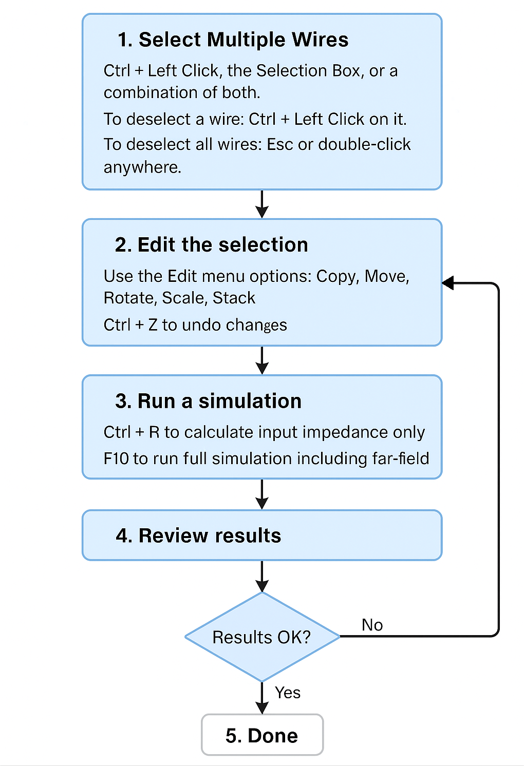
1️⃣ Select Multiple Wires
- Use the Pick Tool with Ctrl + Left Click, the Box Select tool, or both.
- Selected wires are highlighted in light blue.
- To deselect a wire: Ctrl + Left Click on it.
- To deselect all wires: Press ESC or double-click anywhere on the workspace.
2️⃣ Edit the Selection
- Use the Edit menu options: Modify, Move, Rotate, Scale, Copy, Stack.
3️⃣ Run a Simulation
- Press Ctrl + R to calculate input impedance only.
- Press F10 to run the full simulation including far-field results.
4️⃣ Review Results
5️⃣ Continue Editing
- Selected wires remain highlighted after simulation.
- Resume scaling, moving, rotating, etc., without reselecting.
- Use Ctrl + Z / Ctrl + Y to undo/redo changes.
🔁 Iterate as Needed
- Edit, simulate, and fine-tune your model continuously until you achieve the desired result.
🆕 Improved View Adjustments
Modifying the Selected Wires
Once multiple wires have been selected, navigate to Edit > Modify in the main menu to modify them. The Modify command opens a dialog box (see Fig. 4) with three tabs: Attributes, Materials, and Sources/Loads. Use the checkboxes to specify which parameters you want to modify.
In the Attributes tab, the Segments per Wire and Segments per Wavelength options allow for bulk editing of wire segments. These options are mutually exclusive:
- Segments per Wire sets a fixed number of segments for all selected wires.
- Segments per Wavelength sets the number of segments for each wire based on its length in wavelengths, using the shortest wavelength corresponding to the highest frequency specified.
Entering “0” (zero) in the Segments per Wire field will automatically set the number of segments for each wire based on 10 segments per wavelength.
In the Sources/Loads tab, you can remove sources and loads in bulk by selecting “Delete Sources” or “Delete Loads”.
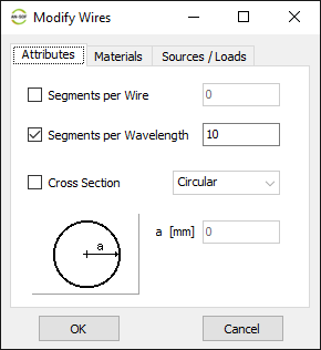
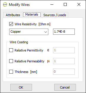
If you need to manipulate the position or arrangement of selected wires, such as moving, rotating, scaling, copying, or stacking them, rather than editing their attributes like the number of segments, cross-section, or material properties, refer to the following articles:
You can delete multiple wires at once by first selecting them using one of the following methods:
- Selection Box – Click and drag a rectangular box around the wires you want to select.
- Wire-by-Wire – Hold down the Ctrl key and left-click on each wire individually.
- Combination – Combine both methods for more flexible selection.
For step-by-step instructions on selecting multiple wires, see the article:
Once the wires are selected, you can delete them using one of the following methods:
- Go to Edit > Delete in the main menu
- Press Ctrl + Del on your keyboard
- Click the Delete button in the toolbar
Figure 1 shows how to select three wires using the Select Wires tool (arrow icon) and Ctrl + left-click, followed by clicking the Delete button in the toolbar.
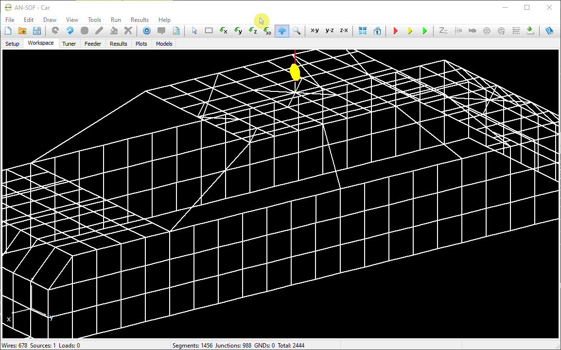
To enable a confirmation prompt before deleting wires, go to Tools > Preferences > Options and check the option “Ask before deleting wires.”
To change the color of a wire, right-click on it to bring up the pop-up menu. Select the Wire Color command to open a dialog box where you can choose a color for the wire. This command is enabled only when a wire is selected.
Alternatively, you can access the Wire Color command by:
- Clicking the Select Wire button (arrow icon) on the toolbar.
- Left-clicking on the wire to select it.
- Navigating to Edit > Wire Color in the main menu.
The Wire Color command is also available as a button on the toolbar.
To change the color of a group of wires (Fig. 1):
- Select the wires using the Selection Box or by selecting them individually (as explained in the section Selecting and Modifying Multiple Wires).
- Navigate to Edit > Wire Color in the main menu.
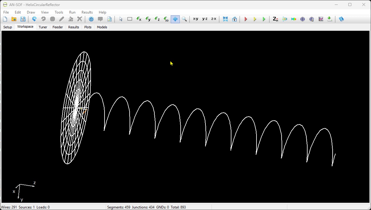
Right-clicking on a wire displays a pop-up menu, where you can select the Wire Properties command.
Alternatively, you can access the Wire Properties command by:
- Clicking the Select Wire button (arrow icon) on the toolbar.
- Left-clicking on the wire to select it.
- Navigating to Edit > Wire Properties in the main menu.
The Wire Properties command is also available as a button on the toolbar.
Executing the Wire Properties command opens the Wire Properties window, which contains three tabs: Geometry, Attributes, and Materials. This window is designed for viewing wire properties only. To edit a wire, refer to the section Modifying a Wire.
The Geometry Tab
This tab displays the geometrical properties of the selected wire (see Fig. 1), including:
- Start Point: Cartesian coordinates of the wire’s start point.
- End Point: Cartesian coordinates of the wire’s end point.
- Wire Length: Length of the wire.
- Segment Length: Length of a wire segment. For curved wires with non-uniform segments, this is the average segment length.
- Shortest Wavelength (λ): Wavelength corresponding to the highest frequency specified in the Frequency panel.
- Wire Length/λ: Wire length measured in wavelengths (based on the shortest wavelength).
- Segment Length/λ: Length of a wire segment in wavelengths (based on the shortest wavelength).
- Segments Per Wavelength: Number of segments the wire would have if its length were one wavelength. This is the inverse of the segment length measured in wavelengths: 1/(Segment Length/λ).
- Hallen’s Parameter (Ω): A parameter that measures wire thickness, defined as Ω = 2 ln(L/a), where L is the wire length and a is the wire radius.
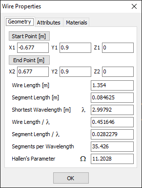
The Attributes Tab
This tab displays the electrical properties of the selected wire (see Fig. 2), including:
- Number of Segments: Number of segments into which the wire is divided.
- Number of Sources: Number of sources placed on the wire.
- Number of Loads: Number of loads placed on the wire.
- Cross-Section: Type and dimensions of the wire’s cross-section.
- Equivalent Radius: Equivalent radius of the cross-section.
- Equivalent Radius/λ: Equivalent radius as a fraction of the shortest wavelength.
- Thin-Wire Ratio: Ratio of the wire diameter to the segment length. This must be less than 3 when the Exact Kernel option is unchecked in the Settings panel of the Setup tab. If the Exact Kernel option is checked, any value of the thin-wire ratio is allowed. For non-circular cross-sections, the wire diameter is twice the equivalent radius.
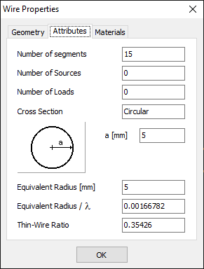
The Materials Tab
This tab displays the material properties of the selected wire (see Fig. 3), including:
- Wire Resistivity: Resistivity of the wire in [Ohm·m]. If the wire is coated, this refers to the resistivity of the internal conductor.
- Wire Coating: Parameters of the wire’s coating shield.
- Relative Permittivity: Permittivity (dielectric constant) of the coating material relative to the permittivity of vacuum.
- Relative Permeability: Magnetic permeability of the coating material relative to the permeability of vacuum.
- Thickness: Thickness of the coating shield.
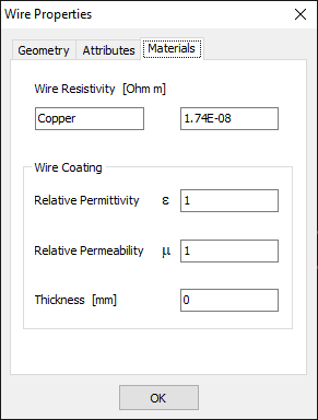
A wire junction is automatically established when the coordinates of a wire end match the end coordinates of a previously added wire. Wire junctions are essential to satisfy Kirchhoff’s current law at the connection point.
Figure 1 illustrates the correct and incorrect ways to connect two wires. To connect the end of wire 1 to a point on wire 2 that is not an end, you must split wire 2 into two wires. This means three wires will be needed instead of two to make the connection.
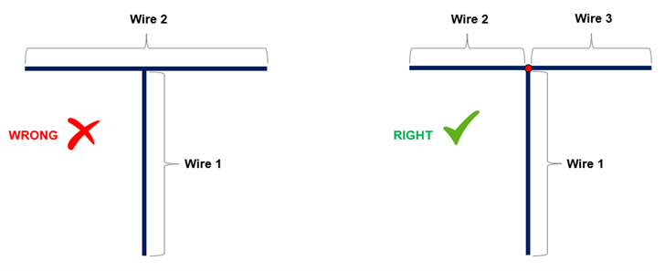
Connecting Wires by Copying and Pasting Ends
Two wires can be connected by copying and pasting their ends:
- Right-click on a wire to select it.
- From the pop-up menu, choose Copy Start Point or Copy End Point to copy the coordinates of the wire end to an internal clipboard.
- Paste the copied point in the Draw dialog box when adding a new wire by clicking the From Point button, located just above the start point coordinates (X1, Y1, Z1) (see Fig. 2).
Note:
- When a wire is selected in the workspace, it will be highlighted in light blue, and an arrow will appear at the End Point. The opposite end is the Start Point.
- Wire orientation serves as the electrical reference for the phase of the current distribution. However, it does not affect observables such as input impedance (and thus VSWR or S11) or radiation pattern metrics (directivity, gain, efficiency, etc.).
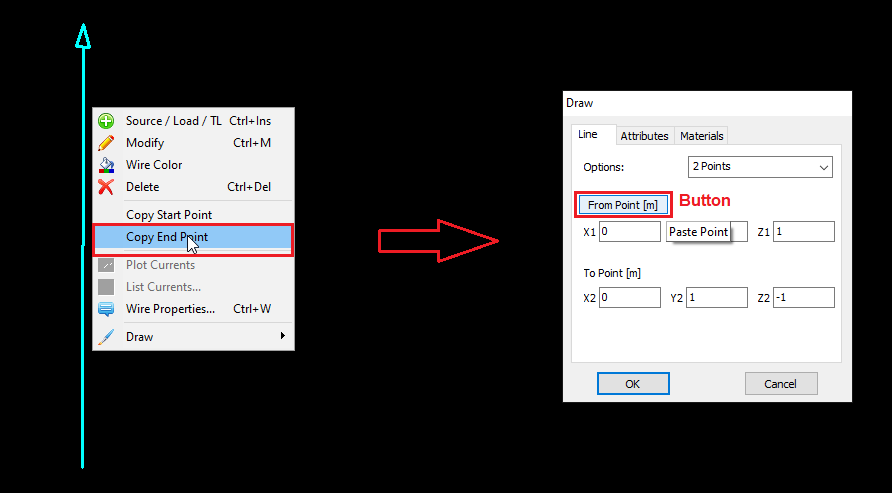
Copying Start and End Points via the Wire Properties Window
The Start and End Points of a wire can also be copied to the AN-SOF internal clipboard for use in a dialog box to draw another wire, using buttons in the Wire Properties window. This procedure is demonstrated in the video below and explained in detail in the following section.
Procedure for Connecting Two Wires at Their Ends
This procedure demonstrates how to connect the Start or End Point of wire #1 to the Start Point of wire #2:
- Right-click on wire #1 to display a pop-up menu.
- Choose the Copy Start Point or Copy End Point command. This command is also available in the Wire Properties window of the selected wire (see Fig. 3).
- In this example, wire #2 will be a Line. Navigate to Draw > Line in the main menu to open the Draw dialog box for the Line.
- Click the From Point button to paste the copied point (see Fig. 4). Then, complete the definition of wire #2.
Using this procedure, any number of wires can be connected at the same point.
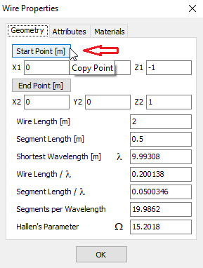
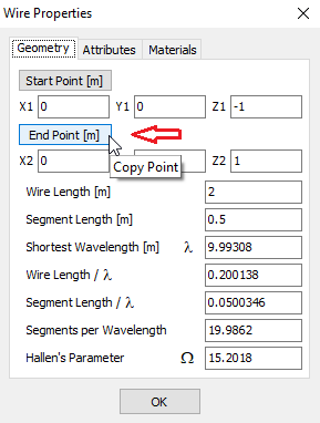
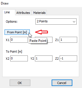
After drawing the wire structure, you may need to adjust the position, orientation, or size of individual wires or groups of wires. To modify wires, you must first select them.
Selecting Wires
- Using the Selection Box:
- Click the Selection Box button on the toolbar.
- Drag a box using the mouse while holding the left button to enclose the wires you want to modify (see Fig. 1).
- Dragging the box from top to bottom selects only fully enclosed wires.
- Dragging the box from bottom to top selects partially enclosed wires as well.
- Enclosing already selected wires with the selection box will deselect them.
- Selecting Wire by Wire:
- Click the Select Wire button (arrow icon) on the toolbar.
- Hold the Ctrl key and left-click on individual wires to select them.
- To deselect a wire, hold the Ctrl key and click on it again.
- To deselect all wires, double-click on the screen or press ESC.
You can also combine the Selection Box method with selecting wires individually.
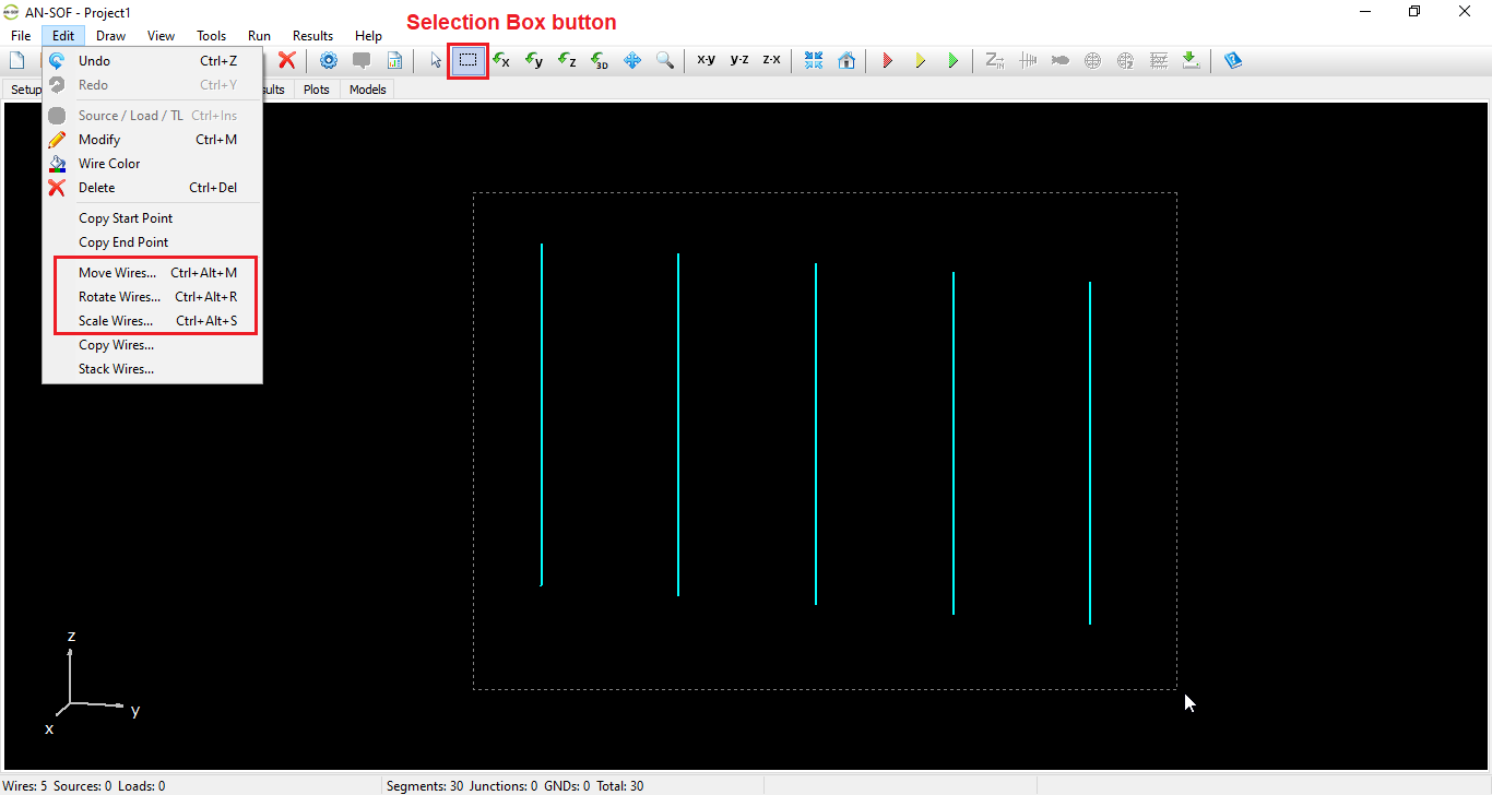
Transforming Selected Wires
Once the wires are selected, navigate to the Edit menu and choose one of the following commands:
Move Wires
Opens the Move Wires dialog box (see Fig. 2), allowing you to move the selected wire or group of wires to a new position. You can specify the shift along the X, Y, and Z coordinates.
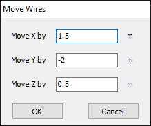
Rotate Wires
Opens the Rotate Wires dialog box (see Fig. 3), enabling you to rotate the selected wire or group of wires around a chosen axis. In addition to the Cartesian axes (X, Y, and Z), the Custom option allows you to define a rotation axis using spherical coordinates (Theta, Phi). You can also set the Rotation Center to rotate around a point other than the origin.
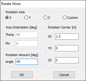
Scale Wires
Opens the Scale Wires dialog box (see Fig. 4), providing the following scaling options:
- Single Factor:
- Apply a single scale factor to all point coordinates of the selected wires.
- Optionally, scale the wire cross-section and coating thickness by the same factor by checking the corresponding boxes.
- Line Length:
- Apply scaling only to linear wires.
- Enter a scale factor and specify an anchored point: the line’s start point (P1) or end point (P2). This allows you to lengthen or shorten the line while keeping one end fixed.
- Advanced:
- Apply different scale factors for each Cartesian coordinate (X, Y, and Z).
- Stretch or contract the selected wires along the direction of one of the Cartesian axes.
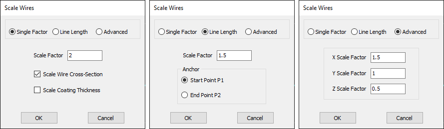
Note
Transmission lines fully enclosed by the selection box will be transformed along with the associated wires when using the Move, Rotate, or Scale transformations in the Edit menu. This ensures that transmission lines remain connected to wires selected via the Selection Box.
When drawing a wire structure, it’s often necessary to copy wires from one position to another—for example, when creating an antenna array. To copy wires, first select them using one of the following methods:
- Click the Selection Box button on the toolbar and drag a box with the mouse to enclose the wires you want to copy (see the Moving, Rotating and Scaling Wires section for details).
- Hold the Ctrl key and left-click on wires to select them individually.
- Combine methods 1 and 2 for more flexible selection.
For a full overview of wire selection techniques, see:
In the Edit menu, you will find the following commands for copying the selected wires:
Copy Wires
Opens the Copy Wires dialog box (see Fig. 1), allowing you to copy the selected wire or group of wires.
- Specify the number of copies of the selected group of wires.
- The first copy will be offset from the original wire group based on the entered X, Y, and Z offsets and/or rotated around each axis according to the entered angles.
- Each subsequent copy will be offset and/or rotated relative to the previous copy.
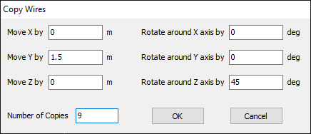
Stack Wires
Opens the Stack Wires dialog box (see Fig. 2), allowing you to stack the selected wire or group of wires along a specified direction.
- Specify the number of elements in the stack. Each “element” consists of the selected wires, which could be a single wire or a group of wires.
- Define the spacing between the elements.
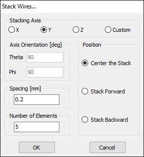
Grids and Surfaces
In AN-SOF, you can model metallic structures using either wire frameworks or solid sheets. Understanding the distinction between these two is key to accurate electromagnetic modeling:
- Wire Grids: These are frameworks composed of interconnected wires with gaps (holes) between them. The wires do not overlap; they meet at junctions to form a mesh.
- Solid Surfaces: These represent continuous, solid metal sheets without holes.
Both grids and surfaces can be constructed using straight or curved segments, allowing for highly complex geometries.
Available Geometries
To create these structures, navigate to Draw > Wire Grid / Solid Surface in the main menu, or use the Drawing Panel (View > Drawing Panel) for faster access.
| Shape | Description |
| Patch | Creates a rectangular surface parallel to the XY-plane. |
| Plate | Creates a flat plate or a “bilinear surface” (a four-sided shape where corners may not be coplanar). |
| Disk | Creates a solid circular plate or a radial wire mesh. |
| Flat Ring | A disk with a central hole (annulus). |
| Cone | A standard conical structure ending in a single point. |
| Truncated Cone | A cone with the top portion removed, resulting in two circular faces of different radii. |
| Cylinder | A traditional cylindrical tube or solid rod representation. |
| Sphere | A full spherical shell modeled as a grid or surface. |
| Paraboloid | Essential for modeling parabolic reflectors and dish antennas. |
Modeling Tips
- The Drawing Panel: We recommend keeping the Drawing Panel open if you are building complex reflectors. It saves several clicks when switching between different primitive shapes.
- Grid Density: When using wire grids to simulate solid surfaces, ensure the “hole” size is small relative to the wavelength (typically less than $\lambda / 10$) to ensure the grid behaves like a solid shield.
The Attributes tab in the Draw dialog box allows you to define how a geometric shape (like a Plate, Disc, or Sphere) is mathematically represented in the simulation. While the shapes differ, they all share the same attribute logic.
Defining the Structure: Wire Grid vs. Solid Surface
The most critical choice is made in the Cross-Section field (Fig. 1). This setting determines whether the object has “holes” or is a continuous sheet of metal.
- Wire Grid: Select Circular cross-section and set a radius ($a > 0$). This creates a mesh of cylindrical wires with open gaps between them.
- Solid Surface: Select Flat or Rectangular cross-section. AN-SOF automatically adjusts the width of these “strip” wires so they touch edge-to-edge, covering the surface completely with no gaps.
- Flat: Represents a surface with zero physical thickness.
- Rectangular: Allows you to specify a physical thickness for the metal sheet.
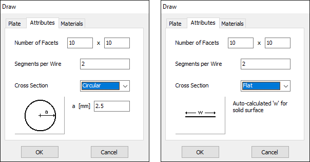
Number of Facets
Facets are the “building blocks” of the grid or surface. They are typically quadrilaterals formed by four interconnected wires.
- Grid Arrangement: You define facets as a grid (e.g., $10 \times 10$ for a Plate or $6 \times 12$ for a Disk).
- Automatic Calculation (Patch only): Setting facets to 0x0 for a Patch allows AN-SOF to auto-calculate the density based on the highest frequency (targeting 10 segments per wavelength).
Segments per Wire
This defines how many computational segments exist on each individual wire that makes up the facets.
- Manual Control: Set a specific integer for custom precision.
- Automatic: Set to zero to let AN-SOF apply the 10-segments-per-wavelength rule.
- Note on Patches: The Patch tool does not have this option because its facets are always composed of single-segment wires.
Individual vs. Mass Editing
Once a grid or surface is created, you have two ways to modify it:
- Mass Edit: Refer to Modifying a Grid/Surface to change the attributes of the entire object at once (e.g., changing the radius of all wires in a mesh).
- Individual Edit: You can right-click any single wire within the mesh to change its specific properties or position without affecting the rest of the grid.
In AN-SOF, wire grids and solid surfaces are treated as collections of individual wires or strips. Once created, they cannot be re-opened in the original “Draw” dialog box. Instead, you use Massive Edition tools to adjust the entire structure at once.
Selecting the Structure
To modify a grid or surface, you must first select the components you want to change:
- The Selection Box: Click the Selection Box button on the main toolbar.
- Draw the Box: Left-click and drag in the workspace to encompass the grid or surface. Selected wires will turn light blue (see Fig. 1).
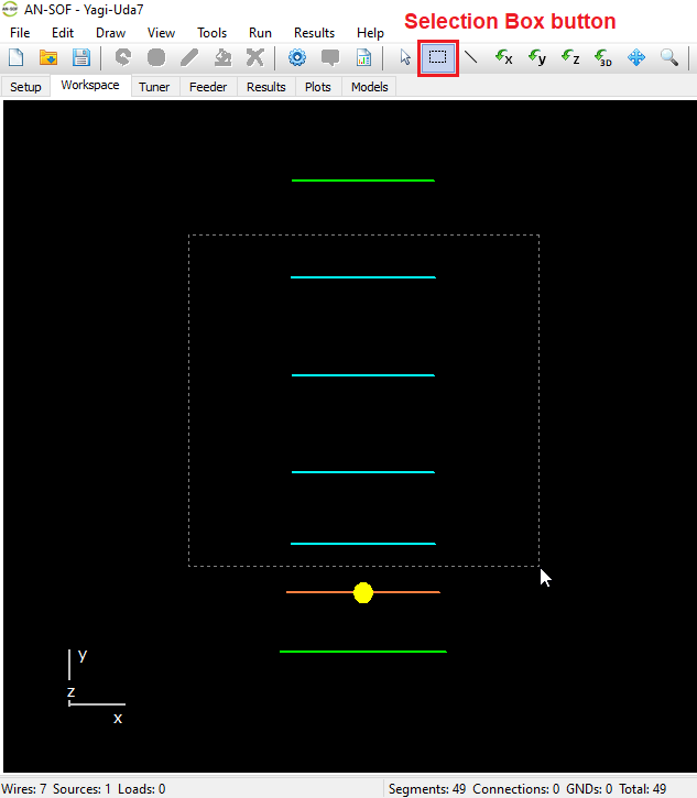
Executing Modifications
Once your selection is highlighted, you can access the modification tools:
- The Modify Command: Go to Edit > Modify, use the shortcut Ctrl + M, or click the Modify button on the toolbar.
- Scope of Changes: This opens a dialog box where you can update the Cross-Section, Resistivity, or Coating for all selected wires simultaneously.
- Refer to: Selecting and Modifying Multiple Wires
Advanced Manipulations
If you need to change the physical orientation or duplicate the structure, use the following specialized commands:
- Move, Rotate, & Scale: Used to reposition a grid (e.g., moving a reflector behind a dipole) or resize it for a different frequency band.
- Copy & Stack: Useful for repeating a grid pattern across an array.
Since wire grids and solid surfaces are composed of numerous individual segments, they must be selected as a group before they can be removed from your project (Fig. 1).
Step-by-Step Deletion
- Activate Selection Mode: Click the Selection Box button on the main toolbar. Refer to: Selecting and Modifying Multiple Wires.
- Define the Area: Left-click in the workspace and drag a box around the grid or surface you wish to remove. All components within the box will be highlighted in light blue.
- Execute Delete:
- Go to Edit > Delete in the main menu.
- Use the keyboard shortcut Ctrl + Del.
- Click the Delete icon on the toolbar.
Important Considerations
- Selective Deletion: Because grids are collections of individual wires, you can choose to delete only a portion of a grid by drawing the selection box around specific segments rather than the whole structure.
- Undo Support: If you accidentally delete the wrong section, you can typically use Ctrl + Z to restore the wires.
- Selection State: The Delete command remains disabled until at least one wire is highlighted.
Changing the color of a grid or surface is an effective way to visually organize complex models, especially when distinguishing between different materials, feed structures, or reflectors.
How to Change the Color
- Select the Structure: Activate the Selection Box tool from the main toolbar. Click and drag to encompass the entire grid or surface. The selected elements will turn light blue (Fig. 1).
- Open the Color Menu:
- Navigate to Edit > Wire Color in the main menu.
- Alternatively, click the Wire Color icon on the toolbar.
- Choose a Color: A standard color picker dialog will appear. Select your desired color and click OK.
This command only becomes active when a selection has been made. If the icon is grayed out, ensure your wires are highlighted in light blue first. Refer to: Selecting and Modifying Multiple Wires.
Benefits of Color Coding
- Material Identification: Use different colors to represent different metals (e.g., Copper wires in orange, Aluminum in gray) to match your resistivity settings.
- Structural Clarity: Color-code your Solid Surfaces (flat strips) differently from your Wire Grids to quickly verify the modeling approach used for each part of the antenna.
- Report Presentation: When exporting screenshots for technical documentation, distinct colors make it much easier for readers to follow your design labels.
Adding Wire Grids/Solid Surfaces
The Patch Command
A Patch in AN-SOF is a specialized tool for creating solid, rectangular conductive surfaces that lie parallel to the XY-plane ($z = \text{constant}$). Unlike a general plate, the Patch is specifically optimized for applications like microstrip antenna design.
Key Characteristics
- Structure: It is composed of flat or rectangular strips that automatically adjust their width to form a continuous, gapless metal sheet.
- Orientation: Always horizontal (parallel to the XY-plane).
- Primary Use Case: Modeling Patch Antennas on a substrate.
- Requirement: To model a patch on a dielectric, you must set the Ground Plane to Substrate by navigating to the Setup tab > Environment panel.
💡 Tip
Patch vs. Plate: Use Patch when your structure is parallel to the ground and you are using the Substrate ground option. Use Plate if you need to model a rectangular surface in free space, above a real ground, or if the surface needs to be tilted or vertical.
Configuration Steps
To open the tool, go to Draw > Wire Grid / Solid Surface > Patch. The dialog box features three tabs:
- Patch Tab: Define the geometry by entering the coordinates of two opposite corner points (X1, Y1) and (X2, Y2) at a specific height (Z) (Figs. 1 and 2).
- Attributes Tab: Specify the Number of Facets.
- If you enter 0x0, AN-SOF automatically calculates the density based on the highest frequency (10 segments per $\lambda$).
- Materials Tab: Assign the resistivity (e.g., Copper) or coating for the metallic sheet.
Automatic Facet Calculation
When the facets are set to 0x0, AN-SOF ensures that the discretization is sufficient for electromagnetic convergence across your entire frequency sweep. This is particularly useful for broadband designs where the electrical size of the patch changes significantly.
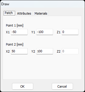
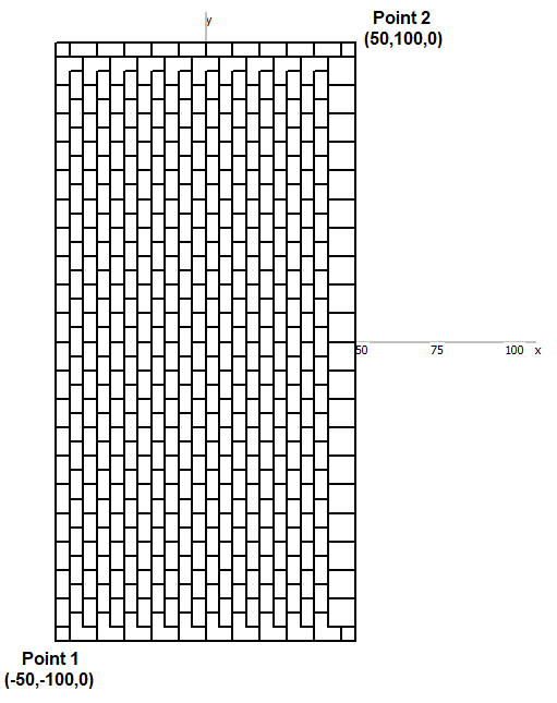
The Plate Command
The Plate command is a versatile tool used to create four-sided metallic structures. Unlike the Patch, which is restricted to the horizontal plane, a Plate can be oriented in any direction or even twisted into a non-planar shape.
Key Characteristics
- Geometry: Defined by four arbitrary vertices in 3D space.
- Bilinear Surface: If the four corner points are not in the same plane, AN-SOF automatically generates a “bilinear surface.” This is a curved quadrilateral where the edges remain straight but the surface itself twists to connect the points.
- Degenerate Case: If all four points are coplanar, the command simply creates a standard flat quadrilateral (rectangle, trapezoid, or rhombus).
- Flexibility: Can be used in free space or above a real ground.
Configuration Steps
To open the tool, navigate to Draw > Wire Grid / Solid Surface > Plate.
- Plate Tab: Enter the (X, Y, Z) coordinates for each of the four corner points (P1, P2, P3, and P4) (see Fig. 1 and 2).
- Attributes Tab:
- Selection: Choose Circular for a wire grid or Flat/Rectangular for a solid metal sheet.
- Facets: Define the grid density (e.g., $N \times M$ facets).
- Materials Tab: Specify the resistivity and any optional insulation or dielectric coating.
Common Use Cases
- Reflectors: Creating tilted or vertical ground planes and corner reflectors.
- Complex Housings: Modeling the metallic chassis of a device where surfaces are not perfectly aligned with the primary axes.
- Aero-structures: Modeling segments of aircraft wings or fuselage where the surface may have a subtle twist or non-planar geometry.
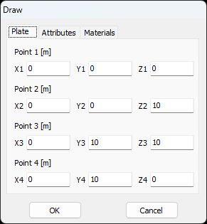
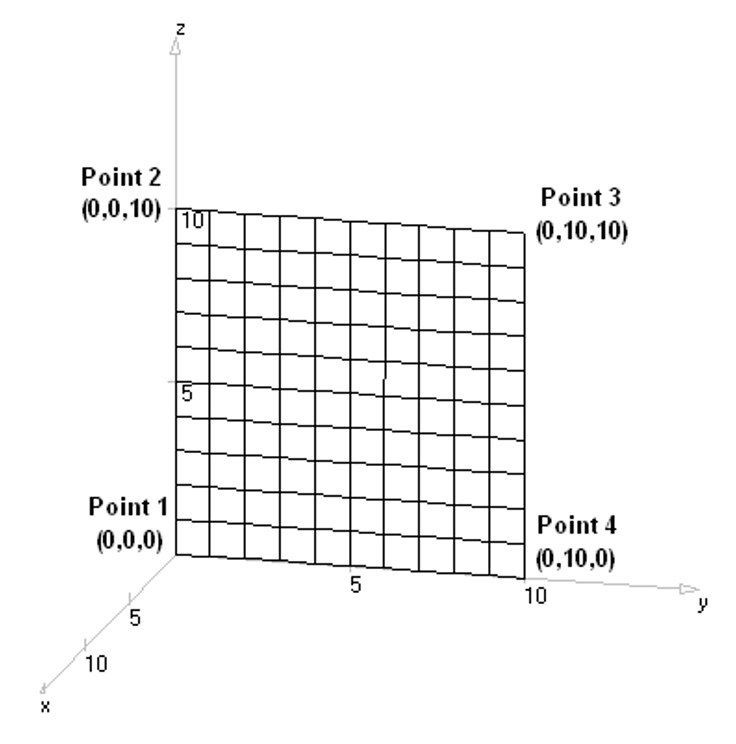
The Disk Command
The Disk command allows you to create circular metallic structures, such as ground planes, circular patch antennas, or reflector elements. Like other surface tools in AN-SOF, it can be modeled as either a transparent wire mesh or a continuous solid sheet.
To open the tool, navigate to Draw > Wire Grid / Solid Surface > Disk.
Geometric Precision: Curved vs. Straight
When setting up your disk, you have two options for how the circular edges are handled:
- Curved Segments: This provides an exact mathematical representation of the disk’s curvature. It is generally recommended for high-frequency simulations where edge effects are critical.
- Straight Segments: This approximates the circle using a series of straight linear wires (creating a polygon). This can be useful for simplifying geometry when exporting to solvers that do not support curved entities.
Orientation and Positioning
To define the disk’s location and “tilt” in 3D space, you use the following parameters:
- Center Coordinates (Cx, Cy, Cz$): The precise origin point of the disk (Figs. 1 and 2).
- Radius: The distance from the center to the outer edge.
- Theta and Phi: These angles define the disk axis direction (the vector perpendicular to the surface). For a disk lying flat on the XY-plane, you would set Theta = 0 deg.
Defining the Facets
In the Attributes tab, you define the density of the disk by specifying the number of Radial and Azimuthal (circular) divisions.
- Radial Facets: The number of divisions from the center to the edge.
- Azimuthal Facets: The number of divisions around the $360^{\circ}$ circumference.
Grid vs. Solid Surface
- Wire Grid: Select Circular cross-section in the Attributes tab to create a “spoke and wheel” radial mesh.
- Solid Surface: Select Flat or Rectangular to create a solid circular sheet. AN-SOF will automatically use flat strips to fill the circular area completely.
Materials
In the Materials tab, you can assign the physical properties of the metal, such as resistivity (e.g., Copper or Aluminum), or apply a dielectric coating if the disk is insulated.
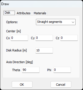
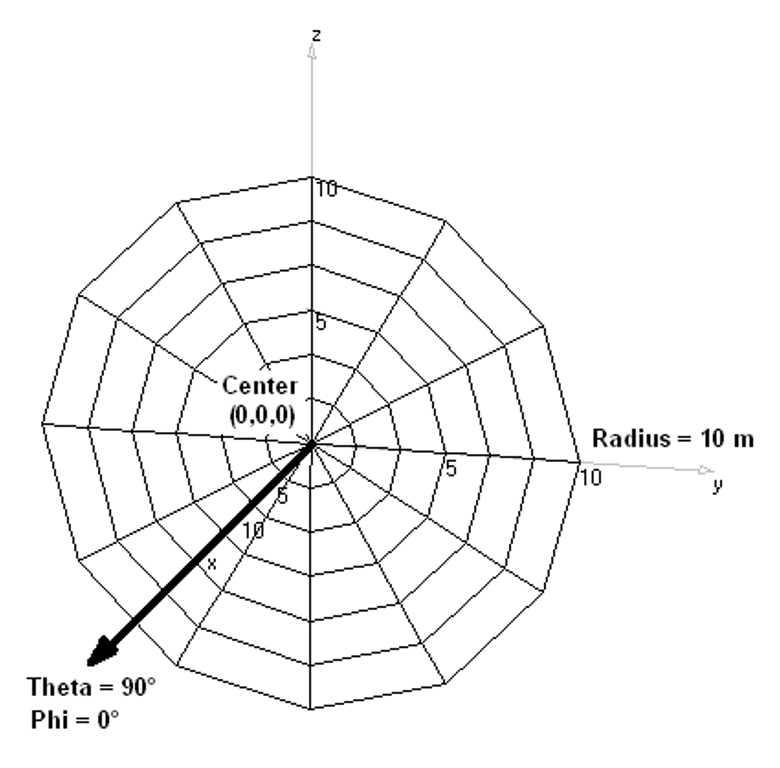
Solid Disk Equivalent Radius Calculator
The Flat Ring Command
The Flat Ring command is used to create an annular (ring-shaped) surface, essentially a disk with a circular hole at its center. This is a common geometry for specialized ground planes, circular loop-fed antennas, or parasitic ring elements.
To open the tool, navigate to Draw > Wire Grid / Solid Surface > Flat Ring.
Geometry and Orientation
To define the physical placement and size of the ring, you provide the following parameters in the Flat Ring tab:
- Center Coordinates (Cx, Cy, Cz): The origin point of the ring’s center (Figs. 1 and 2).
- Radii: You must define both the Inner Radius (the size of the central hole) and the Outer Radius.
- Orientation (Theta and Phi): These angles define the vector perpendicular to the ring’s surface (the ring axis). For example, setting Theta = 0 places the ring on the horizontal XY-plane.
Curvature: Curved vs. Straight
Like the Disk command, you can choose how the software handles the circular edges:
- Curved Segments: Recommended for maximum electromagnetic accuracy, as it uses the exact mathematical curvature of the ring.
- Straight Segments: Approximates the ring circles using a series of straight wire segments (polygonal approximation).
Attributes and Faceting
In the Attributes tab, you determine how the ring is “meshed” for the simulation engine:
- Facets: Define the density of the mesh using Radial (from the inner edge to the outer edge) and Azimuthal (around the circle) divisions.
- Wire Grid vs. Solid Surface:
- Select Circular cross-section to create a wire mesh.
- Select Flat or Rectangular to create a continuous, solid metal sheet. AN-SOF will automatically calculate the strip widths to ensure there are no gaps between the facets.
Materials
In the Materials tab, you can assign the physical properties of the metal, such as resistivity (e.g., Copper or Aluminum), or apply a dielectric coating if the ring is insulated.
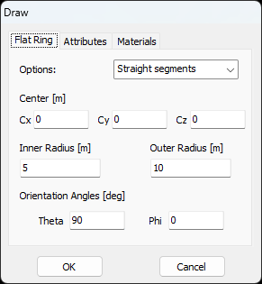
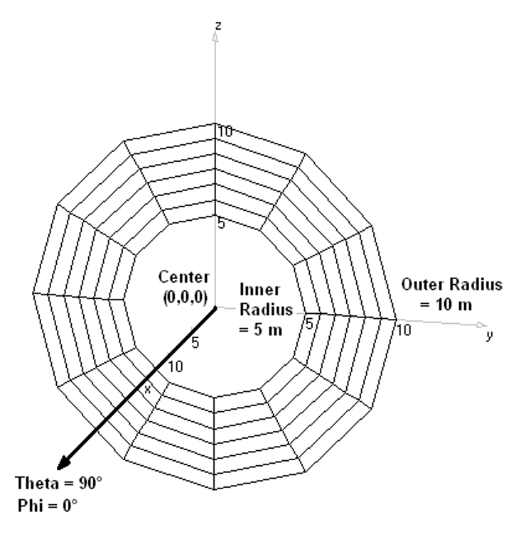
Solid Ring Equivalent Radii Calculator
The Cone Command
The Cone command allows you to create conical metallic structures, which are frequently used in the design of wideband biconical antennas and horn antenna transitions.
To open the tool, navigate to Draw > Wire Grid / Solid Surface > Cone.
Defining the Geometry
In the Cone tab, you configure the physical dimensions and orientation of the structure using the following parameters:
- Vertex Coordinates (Vx, Vy, Vz): The precise point where the cone originates (the tip) (see Figs. 1 and 2).
- Aperture Angle: The full angular opening of the cone.
- Aperture Radius: The radius of the circular base of the cone.
- Orientation (Theta and Phi): These angles define the direction of the cone’s axis (the line passing through the vertex and the center of the base).
Curvature Options
You can choose how the software represents the circular base and the conical walls:
- Curved Segments: Uses exact mathematical curvature. This is preferred for high-precision simulations to avoid the artificial edge effects caused by polygonal approximations.
- Straight Segments: Models the cone as a series of flat triangular or trapezoidal facets using straight wires.
Faceting and Mesh Attributes
In the Attributes tab, you determine the density of the simulation mesh:
- Facets: Define the number of divisions along the Axis (from vertex to base) and Azimuthally (around the circumference).
- Wire Grid: Choosing a Circular cross-section creates a mesh of wires, often used to simulate “caged” biconical antennas.
- Solid Surface: Choosing Flat or Rectangular cross-sections creates a solid metal sheet. AN-SOF automatically adjusts the strip geometry to ensure the cone surface is completely covered without gaps.
Materials
The Materials tab allows you to set the resistivity (e.g., Copper, Aluminum, or Stainless Steel) and any optional dielectric coating for the cone.
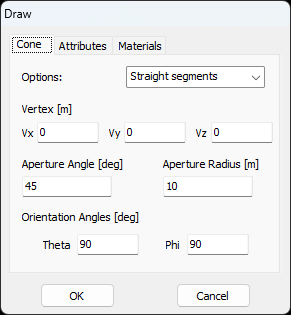
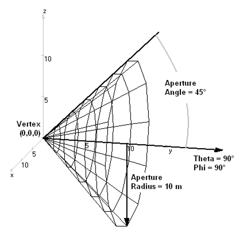
The Truncated Cone Command
The Truncated Cone command allows you to create a “frustum”—a cone with the top portion removed. This versatile tool can be used to model anything from standard conical sections to transitions in horn antennas or even specialized cylindrical supports.
To open the tool, navigate to Draw > Wire Grid / Solid Surface > Truncated Cone.
Defining the Geometry
In the Truncated Cone tab, you configure the physical dimensions and orientation of the structure using the following parameters:
- Base Point Coordinates (Px, Py, Pz): The center of the bottom circular face (Figs. 1 and 2).
- Base Radius & Top Radius: By adjusting these two values, you can create a wide variety of shapes:
- Top Radius ≈ 0: Approaches a standard Cone.
- Top Radius = Base Radius: Creates a Cylinder.
- Different Radii: Creates a standard Truncated Cone.
- Aperture Angle: The angle of the conical slope.
- Orientation (Theta and Phi): These angles define the direction of the central axis connecting the base and top centers.
Curvature Options
- Curved Segments: This provides an exact mathematical representation of the circular edges and the sloped surface. It is recommended for precision modeling to ensure correct current distribution at high frequencies.
- Straight Segments: Approximates the structure using flat facets made of linear wires, forming a polygonal shape.
Faceting and Mesh Attributes
In the Attributes tab, you determine the density of the simulation mesh:
- Facets: Define the number of divisions along the Axis (from base to top) and Azimuthally (around the circumference).
- Wire Grid: Select Circular cross-section to create a “cage” or mesh structure.
- Solid Surface: Select Flat or Rectangular cross-sections. AN-SOF will automatically calculate the necessary strip widths to form a continuous, gapless metallic sheet.
Materials
The Materials tab allows you to set the resistivity (e.g., Aluminum, Brass, or Copper) and apply any optional dielectric insulation to the surface.
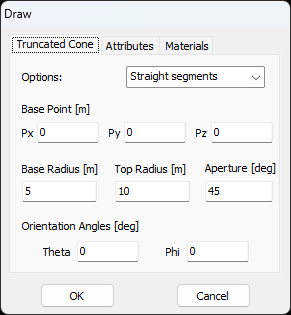
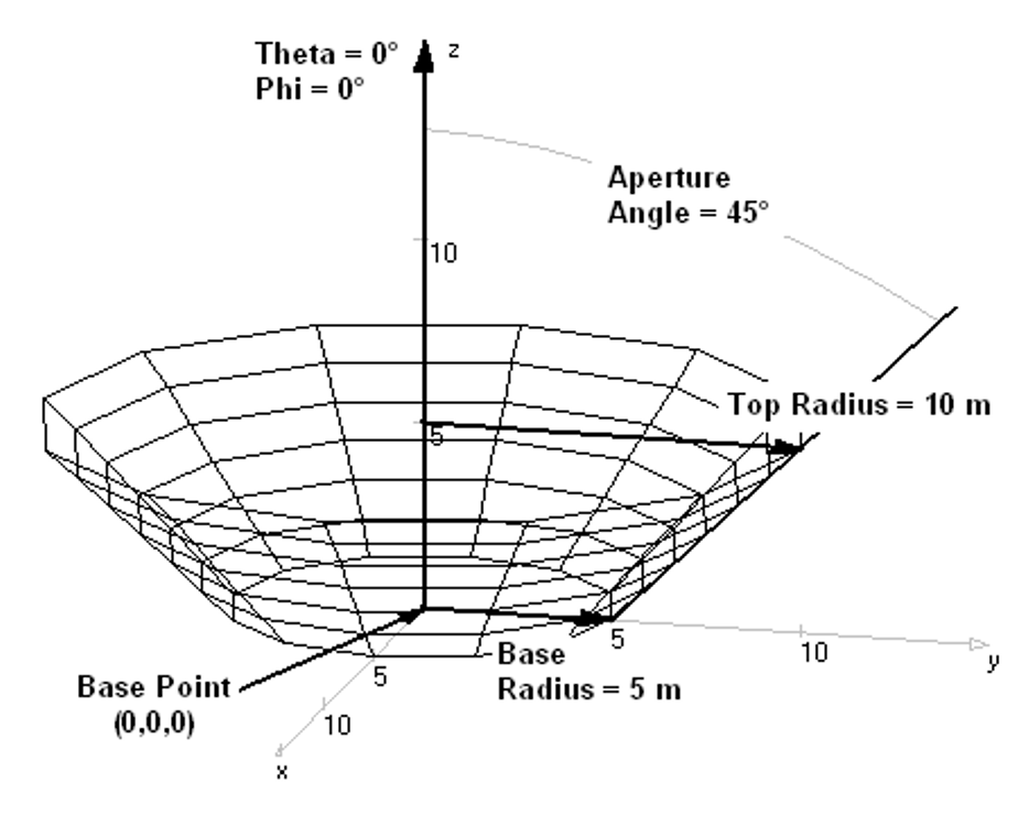
The Cylinder Command
The Cylinder command allows you to create cylindrical conductive structures, which are essential for modeling thick antenna elements, tubular masts, coaxial outer conductors, or shielding cans.
To open the tool, navigate to Draw > Wire Grid / Solid Surface > Cylinder.
Defining the Geometry
In the Cylinder tab, you configure the physical dimensions and spatial orientation of the structure using these parameters:
- Base Point Coordinates (Px, Py, Pz): The center point of the bottom circular face of the cylinder (Figs. 1 and 2).
- Length: The total height of the cylinder along its axis.
- Radius: The distance from the central axis to the outer surface.
- Orientation (Theta and Phi): These angles define the direction of the cylinder’s axis. For a vertical cylinder, you would set Theta = 0 deg.
Curvature Options
You can choose how the software represents the circular cross-section:
- Curved Segments: Provides an exact mathematical representation of the cylinder’s curve. This is highly recommended to ensure the simulation accurately captures surface current distributions.
- Straight Segments: Approximates the cylinder as a prism with a polygonal base.
Faceting and Mesh Attributes
In the Attributes tab, you define the computational mesh:
- Facets: Specify the number of divisions along the Axis (lengthwise) and Azimuthally (around the circumference).
- Wire Grid: Select Circular cross-section to create a “caged” cylinder made of a wire framework.
- Solid Surface: Select Flat or Rectangular cross-sections. AN-SOF will automatically adjust the strip widths to form a continuous, solid metal tube.
Materials
Use the Materials tab to define the resistivity of the cylinder (e.g., Aluminum for a mast or Copper for a high-Q resonator) and to add any dielectric coating or insulation.
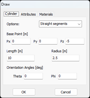
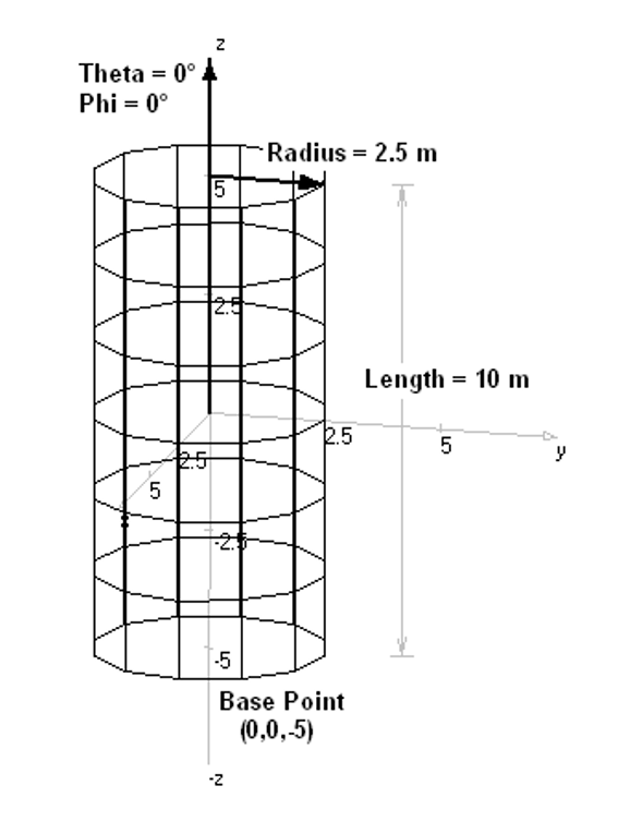
The Sphere Command
The Sphere command allows you to create spherical conductive structures, which are useful for modeling satellite bodies, spherical antennas, scattering targets (RCS studies), or spherical ground systems.
To open the tool, navigate to Draw > Wire Grid / Solid Surface > Sphere.
Defining the Geometry
In the Sphere tab, you configure the physical dimensions and orientation of the sphere using these parameters:
- Center Coordinates (Cx, Cy, Cz): The exact origin point of the sphere.
- Radius: The distance from the center to the surface.
- Orientation (Theta and Phi): While a perfect sphere is symmetrical, these angles define the orientation of the poles (the axis of the azimuthal and polar facets). This is important when you need to align the sphere’s mesh with other connected wires.
Curvature Options
- Curved Segments: This provides an exact mathematical representation of the sphere’s curvature. It is the preferred setting for high-frequency simulations to ensure smooth current flow and accurate scattering results.
- Straight Segments: Approximates the sphere using a series of flat facets made of linear wires, resulting in a polyhedral shape (similar to a geodesic dome).
Faceting and Mesh Attributes
In the Attributes tab, you define the computational density of the sphere:
- Facets: Specify the number of divisions along the Polar (latitude) and Azimuthal (longitude) directions.
- Wire Grid: Select Circular cross-section to create a transparent mesh, often used for “caged” or wire-frame spherical reflectors.
- Solid Surface: Select Flat or Rectangular cross-sections. AN-SOF will automatically calculate the tapering strip widths to ensure the spherical surface is completely covered without gaps.
Materials
The Materials tab allows you to set the resistivity of the sphere (e.g., Silver, Copper, or Aluminum) and to add any optional dielectric coating or insulation.
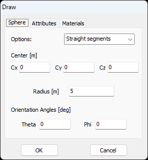
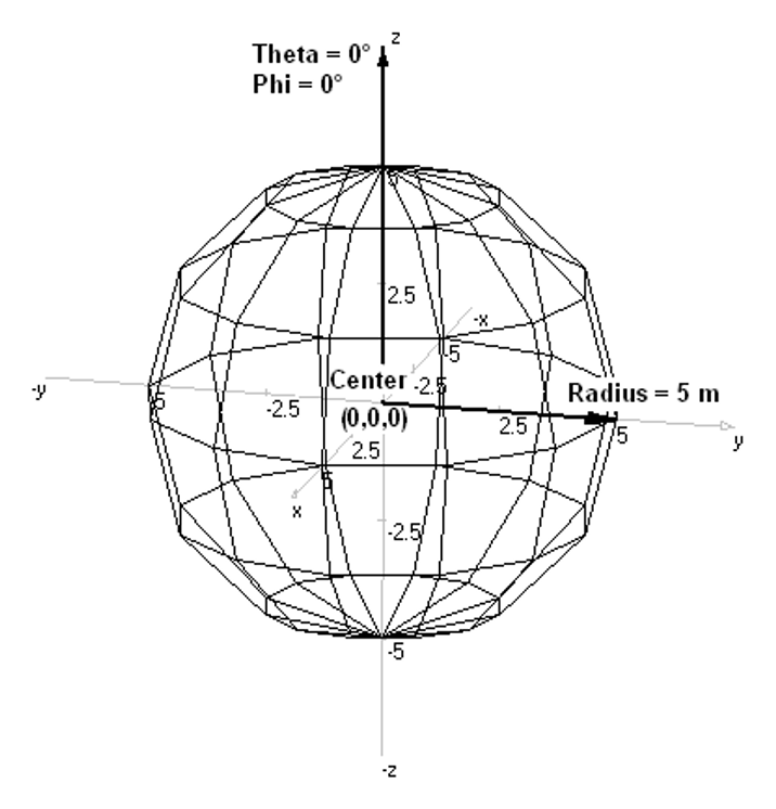
The Paraboloid Command
The Paraboloid command is a specialized tool for creating parabolic reflectors, the most common geometry for high-gain dish antennas used in satellite communications, radar, and radio astronomy.
To open the tool, navigate to Draw > Wire Grid / Solid Surface > Paraboloid.
Defining the Geometry
In the Paraboloid tab, you configure the mathematical curve and physical size of the reflector:
- Vertex Coordinates (Vx, Vy, Vz): The coordinates of the bottom-most point (the center) of the dish (Figs. 1 and 2).
- Focal Length: The distance from the vertex to the focal point where the feed antenna is typically placed. This determines the “deepness” of the dish.
- Aperture Radius: The distance from the central axis to the outer rim of the dish.
- Orientation (Theta and Phi): These angles define the direction of the paraboloid’s axis of symmetry. For a dish pointing directly upward, set Theta = 0 deg.
Curvature Options
- Curved Segments: This utilizes the exact mathematical parabolic curve. It is highly recommended for reflectors, as even small polygonal errors in the surface can lead to significant phase errors in the reflected wave at high frequencies.
- Straight Segments: Approximates the parabolic surface using a series of flat facets made of linear wires.
Faceting and Mesh Attributes
In the Attributes tab, you define the computational density of the reflector:
- Facets: Specify the number of divisions along the Radial (from vertex to rim) and Azimuthal (around the $360^{\circ}$ circumference) directions.
- Wire Grid: Select Circular cross-section to create a “mesh dish.” This is often used for lower-frequency antennas to reduce wind load and weight.
- Solid Surface: Select Flat or Rectangular cross-sections to model a solid metallic dish for maximum gain and front-to-back ratio.
Materials
The Materials tab allows you to set the resistivity of the reflector surface. While most reflectors are modeled as Perfect Electric Conductors (PEC), you can specify materials like Aluminum or Steel to account for ohmic losses in the reflector itself.
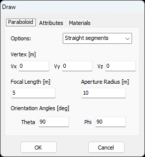
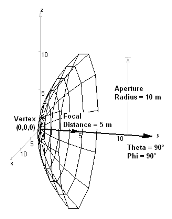
Sources and Loads
Discrete Sources, Incident Field, and Loads
A structure in AN-SOF can be excited either by discrete sources or by an incident electromagnetic field. For the latter, refer to Excitation by an Incident Field. Discrete sources can be placed on any wire segment, and multiple sources may be added, up to one per segment if needed.
A source represents the feed point of a transmitting antenna or an electrical generator. There are two types of sources:
- Voltage sources
- Current sources (used to model impressed currents)
For each source, you must define its amplitude and phase. Additionally, you can assign an internal impedance to simulate non-ideal sources. The impedance can take one of the following forms:
- Series RL (inductive)
- Series RC (capacitive)
- Fixed complex impedance (R + jX)
In addition to sources, lumped loads can be inserted into any wire segment to model passive components or matching circuits. Six types of loads are available:
- Series RL impedance (inductive)
- Series RC impedance (capacitive)
- Fixed R + jX impedance (reactance does not scale with frequency)
- Series RLC circuit
- Parallel RLC circuit
- Trap RLC circuit
To model a pure resistor, set an inductive load with L = 0.
Note:
You can set the units for inductance and capacitance in Main Menu > Tools > Preferences. Supported units include:
• Inductance: pH, nH, µH, mH, H
• Capacitance: pF, nF, µF, mF, F
In the 3D workspace:
- Sources are represented by a yellow circle
- Loads are indicated by a green-highlighted wire segment (see Fig. 1)
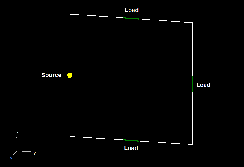
Tips
- To customize the default colors of sources and loads, go to: Main Menu > Tools > Preferences > Workspace tab.
- To change the size of the source displayed in the workspace, go to Main Menu > Tools > Preferences > Workspace tab, and adjust the Source Size % setting.
- Voltage sources have their internal impedance in series.
To model an ideal (perfect) voltage source, set the impedance to zero.
- Current sources have their internal impedance in parallel.
To approximate an ideal current source, use a very high impedance (e.g., 1 MΩ).
Excitation by Sources
To excite the wire structure using discrete sources, go to the Setup tab, open the Excitation panel, and select the Discrete Sources option (see Fig. 2).
If the Set Input Power option is enabled, you can specify the total input power delivered to the structure. In this case, the amplitudes of the voltage and current sources will be automatically adjusted to match the desired input power.
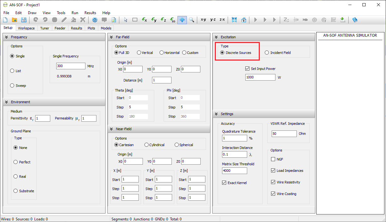
To add a source to a wire segment, first right-click on the desired wire and select “Source / Load / TL (Ctrl + Ins)” from the pop-up menu. A toolbar will appear at the bottom of the screen. Use the slider on this toolbar to select the specific wire segment where you want to place the source.
For more details, see The Source/Load/TL Toolbar.
The Source/Load/TL toolbar is used to connect a source, load, or transmission line to a specific segment of a wire. It also provides tools to edit or remove existing connections.
Accessing the Toolbar
To open this toolbar:
- Right-click on any part of a wire and select Source / Load / TL (Ctrl + Ins) from the pop-up menu (Fig. 1).
- Alternatively, use the main toolbar or go to Edit > Source / Load / TL (Ctrl + Ins) from the main menu. Before using this command, click the Select Wire button (arrow icon on the main toolbar), then left-click the wire where you want to place the source or load.
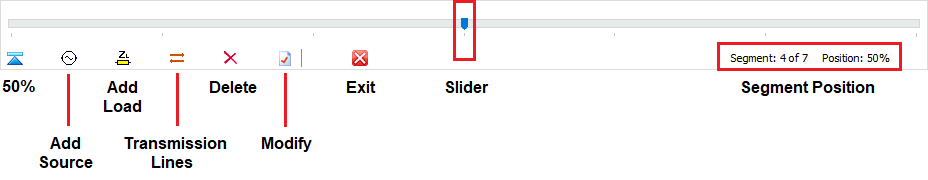
Toolbar Components
Slider
- The slider lets you choose a specific wire segment.
- Each slider position corresponds to a segment along the selected wire.
- On the right side of the toolbar, you’ll see:
- The segment number.
- The segment’s relative position (in %) along the wire, measured from the wire’s starting point to the midpoint of the selected segment:
Segment Position % = 100 × (segment position / wire length)
50% Button
- Quickly positions the slider at the center of the wire.
- Useful for placing sources or loads at the midpoint.
⚠️ Note: The wire must have an odd number of segments for an exact center segment to exist.
Add Source Button
- Opens a dialog box to add a source to the selected segment (Fig. 2).
- You can specify:
- Source type
- Amplitude
- Phase
- Internal impedance Zs
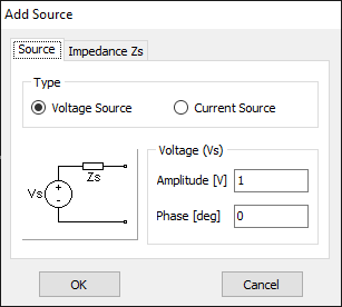
- Voltage sources have their internal impedance in series. To model an ideal (perfect) voltage source, set the impedance to zero.
- Current sources have their internal impedance in parallel. To approximate an ideal current source, use a very high impedance (e.g., 1 MΩ = 1E6 Ohm).
- To change the size of the source displayed in the workspace, go to Main Menu > Tools > Preferences > Workspace tab, and adjust the Source Size % setting.
- To customize the default color of sources, go to: Main Menu > Tools > Preferences > Workspace tab.
Add Load Button
- Opens a dialog to add a load to the selected segment (Fig. 3).
- Load types include:
- Series RL (resistor + inductor)
- Series RC (resistor + capacitor)
- Fixed R + jX impedance (non-frequency-dependent reactance)
- Series or parallel RLC
- Trap (series RL + parallel C)
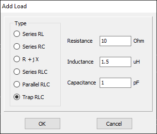
- To customize the default color of loads, go to: Main Menu > Tools > Preferences > Workspace tab.
Transmission Lines Button
- Opens a dialog to connect a transmission line to the selected segment.
- See the section Adding Transmission Lines for more information.
Delete Button
- Removes any existing source or load from the selected segment.
Modify Button
- Opens a dialog to edit the source or load on the selected segment.
Exit Button
- Closes the Source/Load/TL toolbar.
To add a source to a specific wire segment, follow these steps:
- Right-click on any part of the wire to open the pop-up menu.
- Select Source / Load / TL (Ctrl + Ins) to open the Source / Load / TL toolbar at the bottom of the screen (Fig. 1).
- Use the slider to choose the wire segment where the source will be placed.
- Click the Add Source button to open the Add Source dialog box (Fig. 2).
- Specify the type of source, its amplitude (rms value), phase, and internal impedance, then click OK.
- Click Exit to close the Source / Load / TL toolbar.
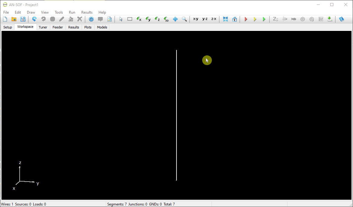
Tips
- To customize the default color of sources, go to: Main Menu > Tools > Preferences > Workspace tab.
- To change the size of the source displayed in the workspace, go to Main Menu > Tools > Preferences > Workspace tab, and adjust the Source Size % setting.
- Voltage sources have their internal impedance in series.
To model an ideal (perfect) voltage source, set the impedance to zero.
- Current sources have their internal impedance in parallel.
To approximate an ideal current source, use a very high impedance (e.g., 1 MΩ = 1E6 Ohm).
To edit an existing source on a wire segment, follow these steps:
- Right-click on any part of the wire to open the pop-up menu.
- Select the Source / Load / TL (Ctrl + Ins) command to open the Source/Load/TL toolbar (Fig. 1).
- Use the slider to locate the segment where the source is placed.
- Click the Modify button to open a dialog box where you can edit the source parameters.
- To remove the source, click the Delete button.
- Click the Exit button to close the Source / Load / TL toolbar.
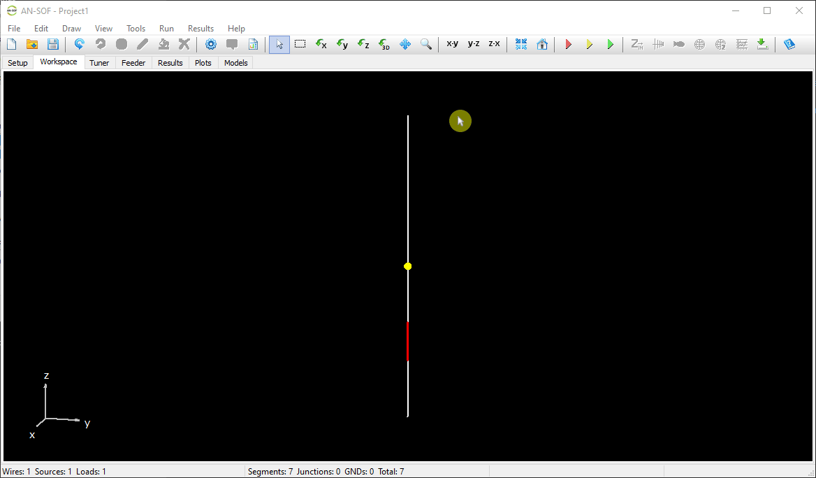
Tips
- To customize the default color of sources, go to: Main Menu > Tools > Preferences > Workspace tab.
- To change the size of the source displayed in the workspace, go to Main Menu > Tools > Preferences > Workspace tab, and adjust the Source Size % setting.
- Voltage sources have their internal impedance in series.
To model an ideal (perfect) voltage source, set the impedance to zero.
- Current sources have their internal impedance in parallel.
To approximate an ideal current source, use a very high impedance (e.g., 1 MΩ = 1E6 Ohm).
To add a load to a selected wire segment, follow these steps:
- Right-click on any part of the wire to display the pop-up menu.
- Select the Source / Load / TL (Ctrl + Ins) command from the menu to open the Source / Load / TL toolbar (Fig. 1) at the bottom of the screen.
- Use the slider on the toolbar to select the desired wire segment.
- Click the Add Load button to open the Add Load dialog box (Fig. 2).
- Specify the load type, along with the required RLC values, then click OK.
- Click the Exit button to close the Source/Load/TL toolbar.
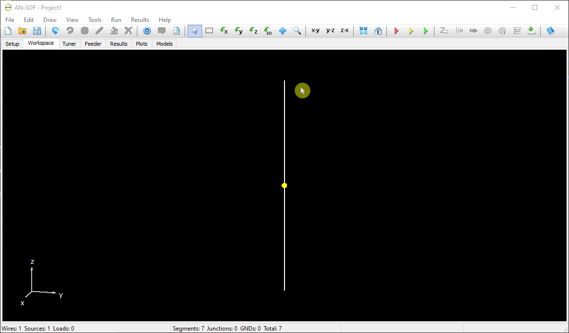
- Load types include (Fig. 2):
- Series RL (resistor + inductor)
- Series RC (resistor + capacitor)
- Fixed R + jX impedance (non-frequency-dependent reactance)
- Series RLC
- Parallel RLC
- Trap (series RL + parallel C)
Tip
- To customize the default color of loads, go to: Main Menu > Tools > Preferences > Workspace tab.
To edit a load on a wire segment, follow these steps:
- Right-click on any part of the wire to open the pop-up menu.
- Select Source / Load / TL (Ctrl +Ins) from the menu to display the Source / Load / TL toolbar (Fig. 1).
- Use the slider on the toolbar to select the segment where the load is located.
- Click the Modify button to open the Edit Load dialog box, where you can update the load’s parameters.
- To remove the load, click the Delete button.
- Click the Exit button to close the toolbar.
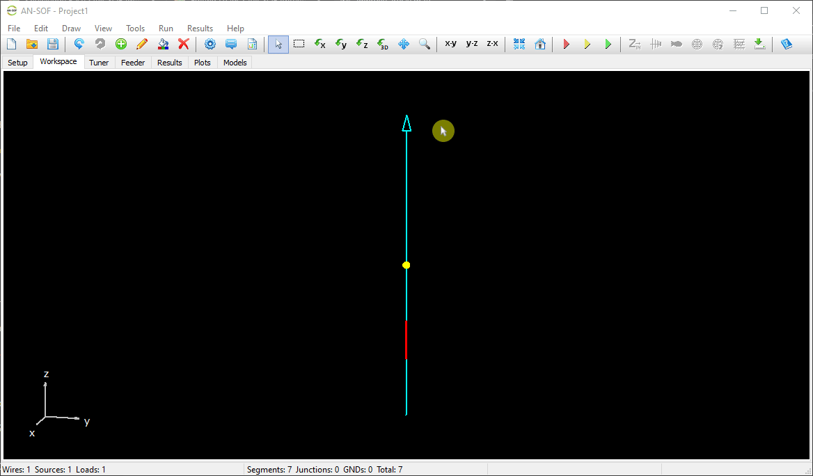
Tip
- To customize the default color of loads, go to: Main Menu > Tools > Preferences > Workspace tab.
You can enable or disable all loads in the simulation without deleting them. This is useful when you want to temporarily exclude load impedances from the analysis.
- Go to the Setup tab and locate the Settings panel in the main window.
- Check or uncheck the Load Impedances option:
- Checked: Loads are enabled and included in the simulation.
- Unchecked: Loads are disabled but remain defined in the model.
See Fig. 1 for reference.
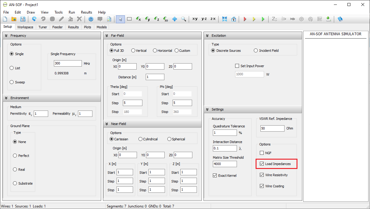
Incident Field
When you want to simulate how an antenna or a metallic structure (like an aircraft or a tower) reacts to external electromagnetic waves, such as for Radar Cross Section (RCS) or scattered field analysis, you use an incident field.
To configure this in AN-SOF:
- Navigate to the Setup tab.
- Locate the Excitation panel.
- Select the Incident Field radio button (Fig. 1).
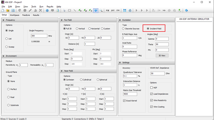
Important Note on Discrete Sources
If you have previously defined discrete sources (voltage or current sources) on specific wire segments, AN-SOF will ignore them once the Incident Field option is active. The structure will be treated as a passive scatterer reacting only to the external plane wave.
Note
When an incident plane wave is used as the excitation, the calculated far-field and near-field results represent the scattered fields. The resulting radiation pattern is the scattered field pattern, observed in the far-field region where the scattered field amplitude decays with the inverse of the distance (1/r), and the scattered power density decays with the inverse square of the distance (1/r²) from the structure.
Once the Incident Field option is selected in the Excitation panel, you must define the characteristics of the incoming plane wave. These parameters determine the wave’s strength, orientation, and polarization.
1. Electric Field & Polarization
- E-Field Major Axis: The amplitude of the incident electric field in V/m (Volts RMS per meter). For linear polarization, this is the field strength. For elliptical polarization, it represents the length of the major axis of the ellipse.
- Axial Ratio: Defines the “roundness” of the polarization.
- 0: Linearly polarized.
- Positive value: Right-handed elliptical polarization.
- Negative value: Left-handed elliptical polarization.
- Gamma ($\gamma$): The polarization angle in degrees. For linear waves, this is the angle between the plane of incidence and the E-field vector. For elliptical waves, it marks the angle to the major axis (Fig. 1).
2. Direction of Arrival
The direction from which the plane wave originates is defined using spherical coordinates:
- Theta ($\theta$): The zenith angle of the incident direction.
- Phi ($\phi$): The azimuth angle of the incident direction.
3. Phase Control
- Phase Reference: The phase of the wave (in degrees) at the coordinate origin $(0,0,0)$. Changing this value simply shifts the phase of all induced currents and scattered fields across the entire structure by the specified amount.
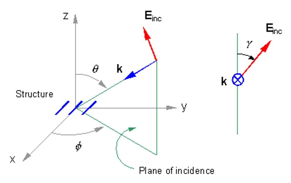
Note
If the incident plane wave option is active, the simulation treats the structure as a passive scatterer. Any defined voltage or current sources are excluded from the calculation.
The 3D-View interface provides an intuitive, graphical method for configuring incident field parameters, allowing you to visualize the direction and polarization of the incoming wave relative to your structure.
Step-by-Step Configuration
- Activate Incident Field: Go to the Setup tab and select the Incident Field option within the Excitation panel.
- Launch the Interface: Click the 3D View button. This opens the 3D-View window along with the Incident Wave dialog box (Fig. 1).
- Adjust Angles: Enter your desired values for Gamma, Theta, and Phi, then press ENTER. Alternatively, you can use the incremental arrows to fine-tune these angles while observing the visual representation in the 3D space.
- Confirm and Sync: Close the Incident Wave dialog box. The values you set graphically are automatically synchronized and will now appear in the Excitation panel of the main interface (Fig. 2).
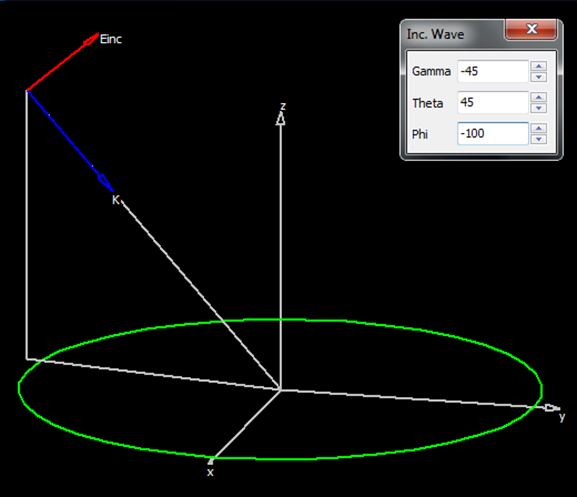
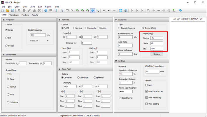
Why Use 3D-View?
Using the graphical interface is highly recommended for complex geometries where the “Plane of Incidence” might be difficult to visualize numerically. It ensures that the Gamma (polarization) angle is oriented exactly as intended relative to the physical orientation of your wires or surfaces.
Ground Planes
A perfectly electric conducting (PEC) ground plane, parallel to the xy-plane, can be added to the model using the following procedure:
- Navigate to the Setup tab > Environment panel.
- Select the Perfect option in the Ground Plane box (see Fig. 1).
- Set the ground plane position under the Position label (Z-coordinate).
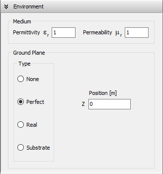
When the Perfect ground is selected, an infinite PEC ground plane will be placed at the specified Z-coordinate relative to the xy-plane:
- If Z > 0, the PEC ground plane will be above the xy-plane.
- If Z = 0, the PEC ground plane will be on the xy-plane.
- If Z < 0, the PEC ground plane will be below the xy-plane.
The ground plane is represented as a square with cross diagonals to visualize its position (see Fig. 2). Note that this is only a symbolic representation, as the ground plane itself is infinite in extent.
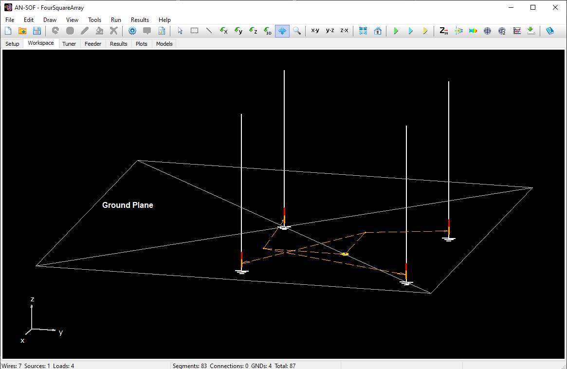
A real (i.e., imperfect or lossy) ground plane, located on the xy-plane (Z = 0), can be added to the model using the following procedure:
- Navigate to the Setup tab > Environment panel.
- Select the Real option in the Ground Plane box (see Fig. 1).
- Specify the Real Ground Option:
- Set the ground Permittivity and Conductivity. If a Radial Wire Ground Screen is selected, also specify the radial length, number of radials, and wire radius.
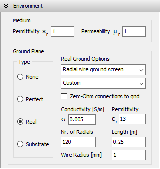
The ground plane is represented as a square with cross diagonals to indicate its position (see Fig. 2). Note that this is only a symbolic representation, as the ground plane itself is infinite in extent. When a Radial Wire Ground Screen is selected, the radial wires lying on the ground will be displayed instead of the ground plane symbol (see Fig. 3).
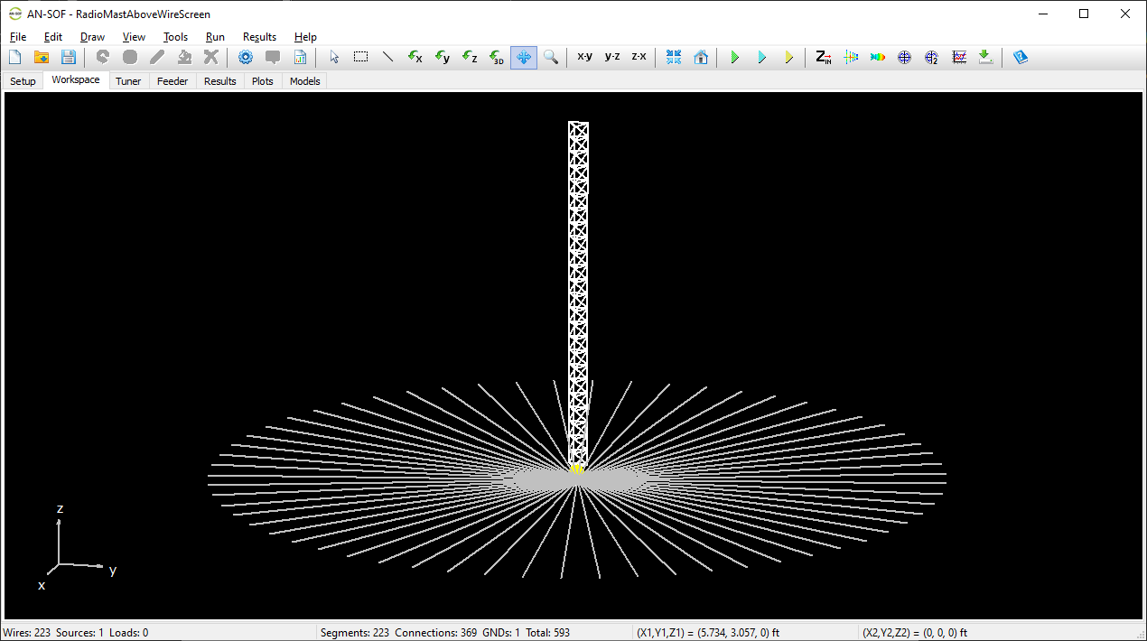
Interactive Ground Model Selection Tools
To help you select the appropriate real ground model, you can use the Loss Tangent Calculator and Ground Plane Selector provided below.
These tools recommend the best ground model for your analysis by considering the wire height, ground connections, operating frequency, and the conductivity $\sigma$ and relative permittivity $\varepsilon_r$ of the soil.
Please remember that these recommendations are intended as a guided starting point. In practical RF engineering, “gray zones” or transition boundaries often exist between theoretical models. If your parameters fall near one of these boundaries, multiple formulations may provide sufficiently accurate results for your specific application.
AN-SOF Loss Tangent Calculator
Calculate the loss tangent of your ground plane to classify its electromagnetic properties and determine the best modeling approach.
AN-SOF Ground Plane Selector
To incorporate a dielectric substrate beneath the xy-plane (Z < 0) into the model, follow these steps:
- Navigate to the Setup tab > Environment panel.
- In the Ground Plane box, select the Substrate option (see Fig. 1).
- Choose between an infinite or finite slab in the Substrate Slab Options box.
- Select a substrate material from the provided list, or choose Custom to specify the substrate’s Permittivity. Set the slab’s Thickness (h) and, if a finite slab is selected, configure its dimensions along the X and Y axes.
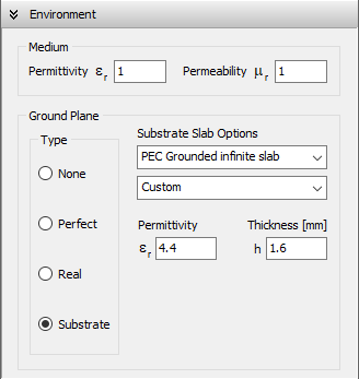
Note:
The substrate slab is backed by a PEC ground plane, which runs parallel to the xy-plane at Z = -h. This ground plane cannot be removed from the simulation (see Fig. 2).
A wire will automatically connect to the ground plane when the z-coordinate of one of its ends coincides with the position of the ground plane.
- When a PEC ground plane is selected, the ground position is specified by the Z value in the Environment panel > Ground Plane box.
- When a real ground is selected, the ground position is Z = 0 (xy-plane).
- When a substrate is selected, a PEC ground plane is placed at Z = -h, where h is the substrate thickness.
Wire connections to the ground plane are indicated with 3D symbols (see Fig. 1).
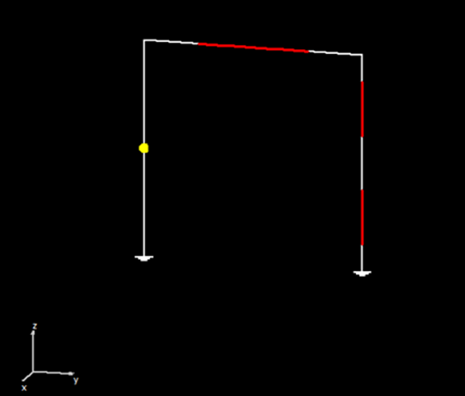
WARNING!
- All wires must be above the ground plane.
- Wires that cross the ground plane from one side to the other are not allowed.
To remove the ground plane, follow these steps:
- Navigate to the Setup tab > Environment panel.
- Select the None (free space) option in the Ground Plane box (see Fig. 1).
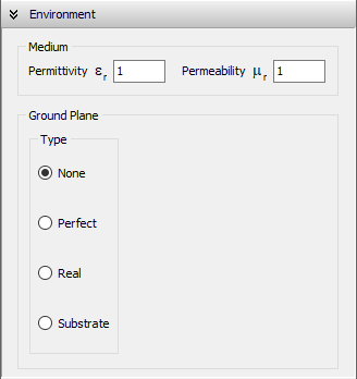
Running Calculations
Once the frequencies, environment, geometry, and excitation are set, AN-SOF is ready to compute the currents flowing on the wire segments.
To calculate the current distribution:
- Navigate to Run > Run Currents (Ctrl + R) in the main menu (see Fig. 1).
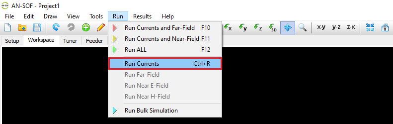
Tip
- When modeling a transmitting antenna and only the input impedance and VSWR/S11 are needed, the Run Currents (Ctrl + R) command saves time by skipping the calculation of the radiated field.
Once the current distribution on the structure has been calculated, the far-field can be computed within the angular ranges specified in the Far-Field panel of the Setup tab.
To calculate the far-field:
- Navigate to Run > Run Far-Field in the main menu (see Fig. 1).
- This command is enabled only after the current distribution has been calculated.
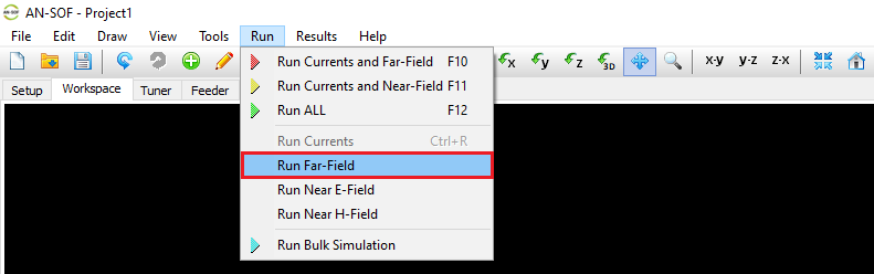
Tip
To sequentially and automatically calculate both the current distribution and the far field, click the Run Currents and Far-Field (F10) button on the toolbar.
Note
When an incident plane wave is used as the excitation, the calculated far-field results represent the scattered field. The resulting radiation pattern is the scattered field pattern, observed in the far-field region where the scattered field amplitude decays with the inverse of the distance (1/r), and the scattered power density decays with the inverse square of the distance (1/r²) from the structure.
Once the current distribution on the structure has been calculated, the near electric field can be computed at the points in space specified in the Near-Field panel of the Setup tab.
To calculate the near electric field:
- Navigate to Run > Run Near E-Field in the main menu (see Fig. 1).
- This command is enabled only after the current distribution has been calculated.
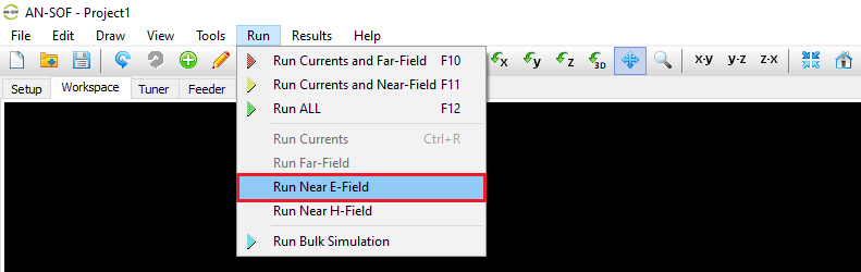
Tips
- To sequentially and automatically calculate both the current distribution and the near fields, click the Run Currents and Near-Field (F11) button on the toolbar. This command also calculates the near H-Field.
- To avoid calculating the H-Field, go to Main Menu > Tools > Preferences > Options and uncheck the “Run ALL” also calculates the H-Field option.
Note
When an incident plane wave is used as the excitation, the calculated near-field results represent the scattered fields.
Once the current distribution on the structure has been calculated, the near magnetic field can be computed at the points in space specified in the Near-Field panel of the Setup tab.
To calculate the near magnetic field:
- Navigate to Run > Run Near H-Field in the main menu (see Fig. 1).
- This command is enabled only after the current distribution has been calculated.
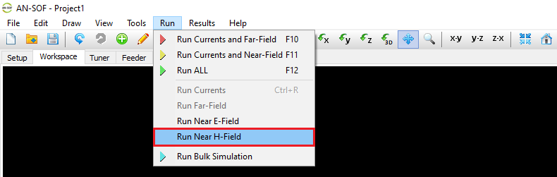
Tips
- To sequentially and automatically calculate both the current distribution and the near fields, click the Run Currents and Near-Field (F11) button on the toolbar. This command also calculates the near E-Field.
- To enable the calculation of the H-Field, go to Tools > Preferences > Options in the main menu and check the “Run ALL” also calculates the H-Field option.
Note
When an incident plane wave is used as the excitation, the calculated near-field results represent the scattered fields.
Once the frequencies, environment, structure geometry, excitation, and far-field observation points have been defined, AN-SOF is ready to perform the calculations. If near-field data is also required, the observation points must first be specified in the Near Field panel. The simulation begins by calculating the current distribution along the wire segments, which also yields the input impedance for a transmitting antenna. The near and far fields are then computed based on these segment currents.
Run ALL (F12) Command
The Run ALL (F12) command allows you to sequentially and automatically calculate the current distribution, far fields, and near fields. To use this command:
- Navigate to Main Menu > Run > Run ALL (F12) (see Fig. 1).
- Alternatively, click the Run ALL button on the toolbar.
Alternative Commands
- If the near field is not required, you can calculate only the currents and far fields by clicking Run > Run Currents and Far-Field (F10). This command is also available on the toolbar.
- If the far field is not required, you can calculate only the currents and near fields by clicking Run > Run Currents and Near-Field (F11). This command is also available on the toolbar.
Separate Calculations
The currents, far fields, and near fields can also be computed separately, as explained in the following articles:
- Calculating the Current Distribution
- Calculating the Far Field
- Calculating the Near E-Field
- Calculating the Near H-Field
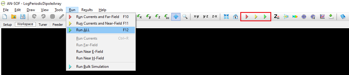
When a calculation is executed using the commands under the Run menu, the Processing window will be displayed (see Fig. 1). This window includes a button to abort the calculation at any time.
Note:
You will be prompted to save the project before aborting, as AN-SOF will restart after the process is terminated.
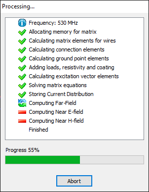
In simulations where the excitation of the structure needs to be changed frequently—such as adjusting the amplitudes of discrete sources or altering the direction of arrival of an incident field—the Numerical Green’s Function (NGF) option can save significant computation time. To enable this option, navigate to the Settings panel of the Setup tab, as shown in Fig. 1.
How NGF Works
- During an NGF calculation, the LU-decomposed matrix of the system is stored in a file after the initial computation.
- Subsequent calculations reuse this stored matrix, allowing them to be performed much faster than the initial one.
Automatic NGF Activation
- When transmission lines are included in the model, the NGF option is automatically enabled.
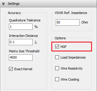
AN-SOF can import a sequence of input files to generate a corresponding sequence of output files, all without requiring user intervention during the process. The input files must adhere to the NEC format and have a .nec extension. The supported NEC commands for importing wires are described in the section: Importing Wires.
Output Data
The output data includes:
- Power Budget or RCS (Radar Cross Section).
- Input Impedances.
- Far Field and Near Fields.
All output data is provided in CSV format. For each NEC input file, AN-SOF generates an individual project containing .emm and .wre files (see File Formats). This allows each project to be opened separately after the bulk simulation is completed.
Initiating a Bulk Simulation
- Navigate to the main menu and select Run > Run Bulk Simulation.
- A prompt will appear, asking if you want to save changes in the current project, as the bulk simulation requires closing the currently open project.
- A dialog box will be displayed, allowing you to select a directory and the input .nec files.
- After selecting the desired files and clicking the Open button, the bulk simulation will begin. The input files will be imported and computed one after another in alphabetical order.
Generated Files
For an input file named “InputFile.nec”, the following files will be generated:
AN-SOF Project Files
- InputFile.emm: Main project file (can be opened with AN-SOF).
- InputFile.wre: Geometry data (wires, segments, connections).
- InputFile.txt: Comments.
- InputFile.cur: Current distribution.
- InputFile.pwr: Input and radiated powers, directivity, gain, etc.
- InputFile.the: Theta component of the far field.
- InputFile.phi: Phi component of the far field.
- InputFile.nef: Near electric field.
- InputFile.nhf: Near magnetic field.
Output CSV Files with Results
- InputFile_PowerBudget.csv: Input and radiated power, efficiency, gain, etc.
- InputFile_Zin.csv: Input impedances, VSWR, S11, etc.
- InputFile_FarFieldX.csv: E-theta and E-phi far field components.
- InputFile_EFieldX.csv: Near electric field components.
- InputFile_HFieldX.csv: Near magnetic field components.
Note:
- “X” represents the frequency in Hz (e.g., X = 300000000 for a frequency of 300 MHz).
- A FarField, EField, and HField file will be generated for each frequency if a frequency sweep simulation has been configured.
Automating Parameter Variations
Bulk simulations automate the calculation process for multiple NEC files, even if they are unrelated, eliminating the need for manual calculations file by file. They are particularly useful for sequentially running calculations on NEC files generated with varying geometric parameters for an antenna. The results can then be analyzed by reading data from the generated CSV files.
For example, you can create a script to generate a sequence of NEC files for a Yagi-Uda antenna, where the spacing between its elements varies. To learn how to accomplish this and read the output data from the CSV files, refer to the following article: Element Spacing Simulation Script for Yagi-Uda Antennas.
Displaying Results
Simulation output in AN-SOF can be analyzed through detailed tabular lists or interactive graphical displays. All data is accessible via the Results menu, organized into five primary analytical groups.
Commands to Display Results
Current Distribution and Impedance
- Current Distribution 3D: Plots the current along the wire structure in a colored 3D view.
- Current Profile 2D: Displays a plot of the current distribution along a selected wire.
- Current vs. Freq: Provides tabulated data of current vs. frequency in a specific wire segment.
- Export Current Data: Saves current data along a selected wire in a TXT or CSV file for external post-processing.
- Input Impedance Table: Tabulates the antenna input impedance, $Z_{in}$ (Resistance and Reactance), and VSWR/S11 across the frequency range.
Far-Field Analysis
- Plot Far-Field Pattern: Displays radiation patterns in 2D (Polar/Rectangular) or 3D.
- Plot Far-Field Spectrum: Shows how field parameters change at a fixed point across frequencies.
- List Far-Field Pattern/Spectrum: Provides the raw numerical data for the patterns and spectra.
- Power & Scattering Metrics: Summarizes input power, radiated power, and efficiency, or the Radar Cross Section for scattering problems.
Near E-Field and H-Field
- Plot Near Field Pattern/Spectrum: Visualizes the Electric ($E$) or Magnetic ($H$) fields in close proximity to the antenna.
- List Near Field Pattern/Spectrum: Tabulates the vector components and magnitudes of the near fields.
Power Density
- Plot/List Power Density Pattern/Spectrum: Analyzes the electromagnetic power flow (Poynting vector magnitude) in either the near or far-field regions.
Data Interpretation: Lists vs. Plots
AN-SOF differentiates between spatial and frequency-based data to provide a comprehensive analysis:
- Tabular Lists: Currents and input impedances are tabulated as a function of frequency.
- Fields (Pattern vs. Spectrum):
- Pattern: Field values at a fixed frequency plotted against a range of observation points (spatial distribution).
- Spectrum: Field values at a fixed observation point plotted against the frequency range (frequency response).
The AN-SOF Visualization Suite
The software includes four specialized tools to handle these results:
- AN-XY Chart: For rectangular plots of spectra and patterns.
- AN-Smith: Dedicated environment for impedance matching and Smith Chart analysis.
- AN-Polar: For 2D polar representations of radiation patterns.
- AN-3D Pattern: For full spatial visualization of lobes and field distributions.
Tip
You can quickly access the most critical results for transmitting antennas, such as Gain, Efficiency, and VSWR, directly in the Metrics tab of the main window without opening secondary applications.
The Metrics tab in the AN-SOF main window (Fig. 1) displays a table with the primary metrics for a transmitting antenna, including:
- Input Impedance (Zin = Rin + jXin)
- VSWR
- S11
- Directivity
- Gain
- Radiation Efficiency
- Horizontal (H) and Vertical (V) Front-to-Rear (F/R) and Front-to-Back (F/B) Ratios
This table is automatically populated only when the wire structure is excited by a discrete source. It will not be filled if the excitation is an incident wave.
The tabulated metrics persist until a new calculation is performed, allowing you to reference them at any time, even when making changes to the project. To export these metrics to a CSV file, click the Export Frequency Metrics button on the toolbar (Fig. 1).
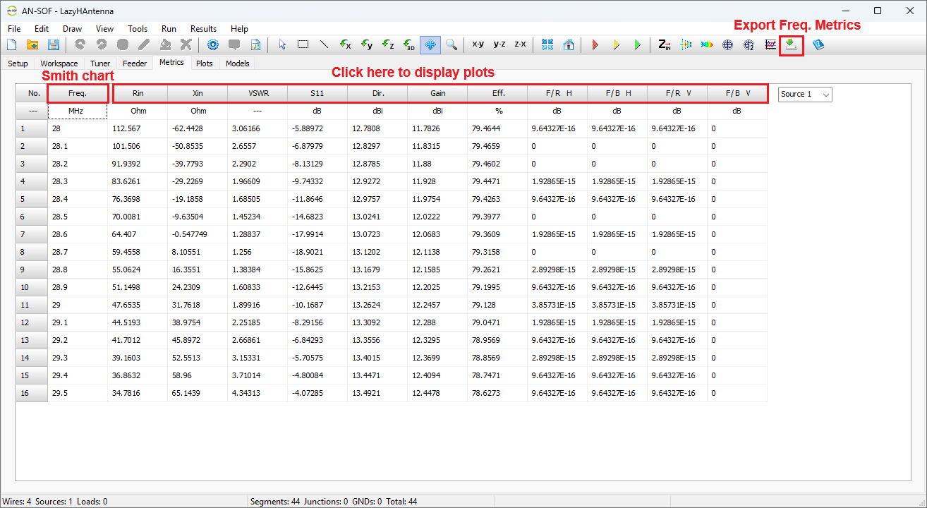
Interactive Column Headers
The column headings, from Rin through F/B V, are interactive buttons (see Fig. 1). Clicking on them displays rectangular plots, where the data in the column is plotted as a function of frequency.
- Click the “Freq.” column header to display the input impedance (Zin = Rin + jXin) in a Smith Chart. By default, this is the input impedance at the antenna feedpoint.
- If the antenna has a feeder and/or tuner connected to its terminals, the impedance seen at the feeder input or tuner input can also be tabulated in the Metrics tab. These can be plotted against frequency in rectangular or Smith charts by clicking the corresponding column headers.
Plotting Impedance at Different Points
- Navigate to the Plots tab > “Zin” box (see Fig. 2) and choose between Antenna, Feeder, or Tuner.
- Go to the Metrics tab, where Rin, Xin, VSWR, and S11 will be tabulated for the selected option (antenna, feeder, or tuner input).
- Click the header buttons as indicated in Fig. 1 to plot these metrics against frequency.
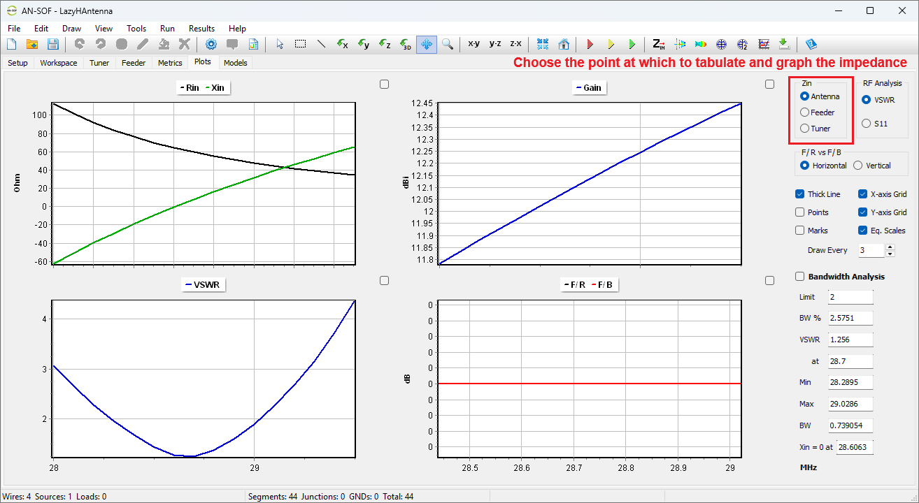
Select the Plots tab in the AN-SOF main window to visualize the plots of the main results for a transmitting antenna as a function of frequency, as shown in Fig. 1. These results are derived from the table in the Results tab.
Plot Layout
- Left Column: Displays the real and imaginary parts of the input impedance (Zin = Rin + jXin) and the VSWR.
- Right Column: Shows the antenna gain in dBi and the Front-to-Rear (F/R) and Front-to-Back (F/B) ratios in dB.
The plots are aligned vertically to facilitate easy comparison.
Customizing Plots
Use the controls on the right side of the Plots tab to adjust various aspects of the graphics, including:
- Line thickness.
- Visualization of points and marks.
- Scales and axes.
- Selection between VSWR or S11.
- Choice between Horizontal (H) or Vertical (V) F/R and F/B ratios.
Each plot can be maximized by clicking the Maximize checkbox located in its upper-right corner.
Input Impedance and VSWR/S11 Options
The input impedance and VSWR/S11 plots can represent:
- The antenna input impedance.
- The feeder + antenna input impedance.
- The tuner input impedance.
The tuner and feeder can be configured in their corresponding tabs next to the Results tab. Whenever a tuner or feeder parameter is changed, the recalculated results in the Results and Plots tabs can be refreshed by selecting the desired option under the Zin box (highlighted in Fig. 1).
Tuner Option
If the Tuner option is selected:
- The input impedance of the tuner will be displayed.
- If the tuner is connected to a combination of feeder + antenna, the input impedance and VSWR/S11 of the tuner + feeder + antenna system will be displayed.
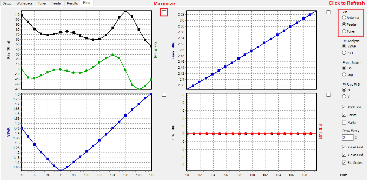
Current Distribution
3D Plots
To visualize how current flows across your entire model, navigate to Results > Plot Current Distribution in the main menu. This command launches the AN-3D Pattern application, which renders the current amplitude directly on the 3D structure using a dynamic color scale (Fig. 1).
Beyond amplitude, you can also analyze the complex components of the current. By selecting the Plot menu within AN-3D Pattern, you can display:
- Amplitude
- Phase
- Real part
- Imaginary part
Adjusting the Color Bar in AN-3D Pattern
For precise data interpretation and professional presentations, you can manually override the automatic scaling. This allows you to set specific increments (e.g., multiples of 5).
- Navigate to Edit > Preferences in the AN-3D Pattern menu (Fig. 2).
- Manually define the Max and Min values of the color scale to highlight specific ranges of interest.
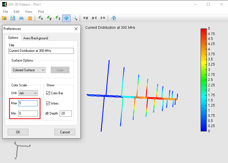
2D Plots
If you need to analyze the current along a specific wire in detail, you can generate a Cartesian plot using AN-XY Chart.
Method 1: Quick Access
Right-click directly on a wire in the workspace and select Plot Currents from the pop-up menu (Fig. 3).
Method 2: Toolbar Selection
- Click the Select Wire button (arrow icon) on the toolbar.
- Left-click the desired wire.
- Go to Results > Plot Currents in the main menu.
Within the AN-XY Chart interface, you can toggle between amplitude, phase, and complex parts via the View menu.
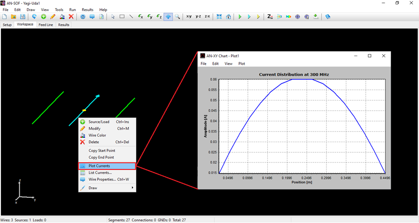
Tips
To optimize your analysis of 2D current distributions, AN-XY Chart provides several interactive navigation and data management features:
- Zooming: To focus on a specific area of the plot, press and hold the left mouse button while expanding a box over the desired region.
- Panning: To move the view without changing the zoom level, right-click on the graph and drag the mouse.
- Reset View: To quickly return to the original full-scale view, left-click and expand a small rectangle in an upward direction anywhere on the plot.
- Units and Export: The main menu offers options to change the units of the plotted magnitudes (e.g., from linear to dB). You can also export the data to external formats for further processing in third-party software.
The List Currents toolbar provides a localized view of electrical data for specific points on your model, allowing for detailed frequency-response analysis.
Accessing the Toolbar
There are two primary ways to access this tool:
- Right-Click Menu: Right-click directly on a wire in the workspace and select the List Currents command from the pop-up menu.
- Main Menu: Click the Select Wire button (arrow icon) on the toolbar, left-click the desired wire, and navigate to Results > List Currents. This option becomes available once the current distribution calculation is complete.
Key Functionalities
The toolbar enables you to pinpoint a specific segment within the selected wire to analyze the following data versus frequency:
- Current Analysis: View the current magnitude and phase for any individual segment.
- Source and Load Data: If the selected segment contains a source or load, the toolbar can display a comprehensive list of parameters:
- Input Impedance
- Voltages and Power levels
- Reflection Coefficient and VSWR
- Return and Transmission Losses
Components of the List Currents Toolbar
The List Currents toolbar provides specific controls to navigate wire segments and analyze their electrical properties across the frequency sweep (Fig. 1).

Navigation Controls
- Slider: Move the slider to select a specific segment along the wire. Each position corresponds to a segment index.
- Segment Number: Displays the index of the currently selected segment.
- Segment Position %: Shows the relative position from the wire’s start to the segment midpoint. It is calculated as:
- $\displaystyle \text{Segment Position \%} = 100 \times \left( \frac{\text{segment position}}{\text{wire length}} \right)$
- 50% Button: Instantly moves the slider to the exact midpoint of the wire. This is particularly useful for verifying or placing center-fed sources and loads.
⚠️ Note: The wire must have an odd number of segments for an exact center segment to exist.
Data and Analysis Buttons
- Current on Segment: Opens a dialog box showing a frequency list of the current for the active segment. Click Plot to generate a frequency-domain graph of the current (Fig. 2).
- Input List: Enabled only if the selected segment contains a source. This dialog displays input impedance, currents, voltages, and powers (Fig. 3).
- Plot: Graph the selected parameter vs. frequency.
- Smith: Visualize input impedance on a Smith Chart.
- Export: Save the data as a CSV file.
- Source List: Enabled when a source is present. It lists currents, voltages, and powers specifically within the internal impedance of the source. Data can be plotted or exported to CSV (Fig. 4).
- Load List: Enabled if the segment contains a load. It displays load impedances, currents, voltages, and powers. Like the other lists, these values can be plotted against frequency or exported (Fig. 5).
- Exit Button: Closes the toolbar and returns to the standard workspace view.
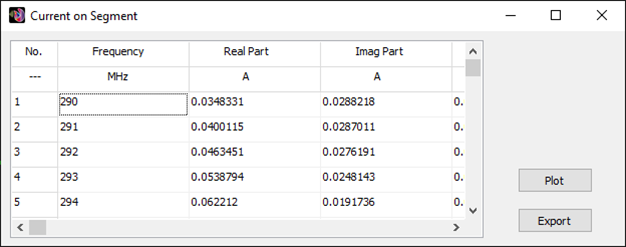
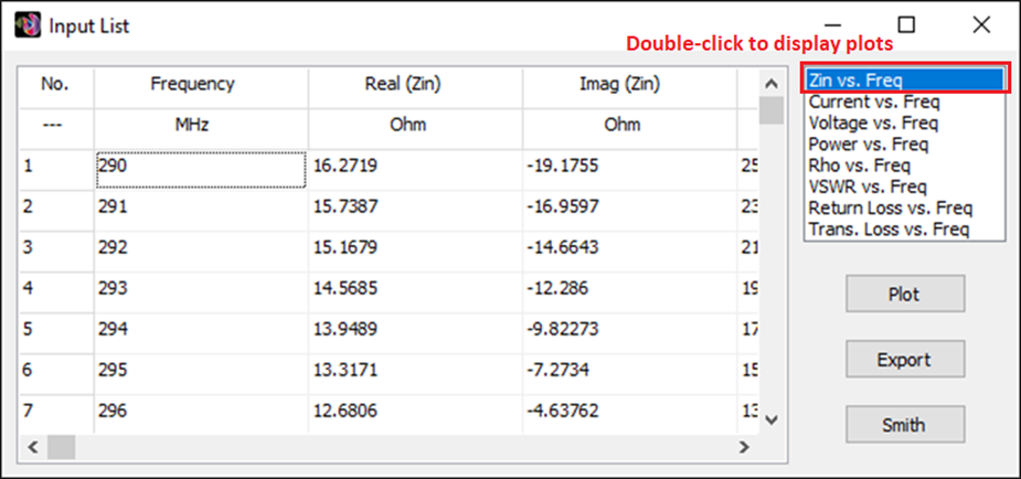
To analyze how the current at a specific point on your antenna behaves across a range of frequencies, follow this procedure:
- Select the Wire: Right-click on the desired wire in the workspace to open the pop-up menu.
- Open the Toolbar: Click the List Currents command. The List Currents toolbar will appear at the bottom of the interface (Fig. 1).
- Target the Segment: Move the slider to navigate through the segments of the selected wire. You can use the 50% button to jump to the center or watch the Segment Position % display to find a specific location.
- View Frequency Data: Click the Current on Segment button. This opens a dialog box that tabulates the current data for every frequency step in your simulation. The table includes:
- Amplitude
- Phase
- Real Part
- Imaginary Part
- Generate a Plot: Click the Plot button within the dialog box to launch AN-XY Chart, where you can visualize the current magnitude or phase as a function of frequency.
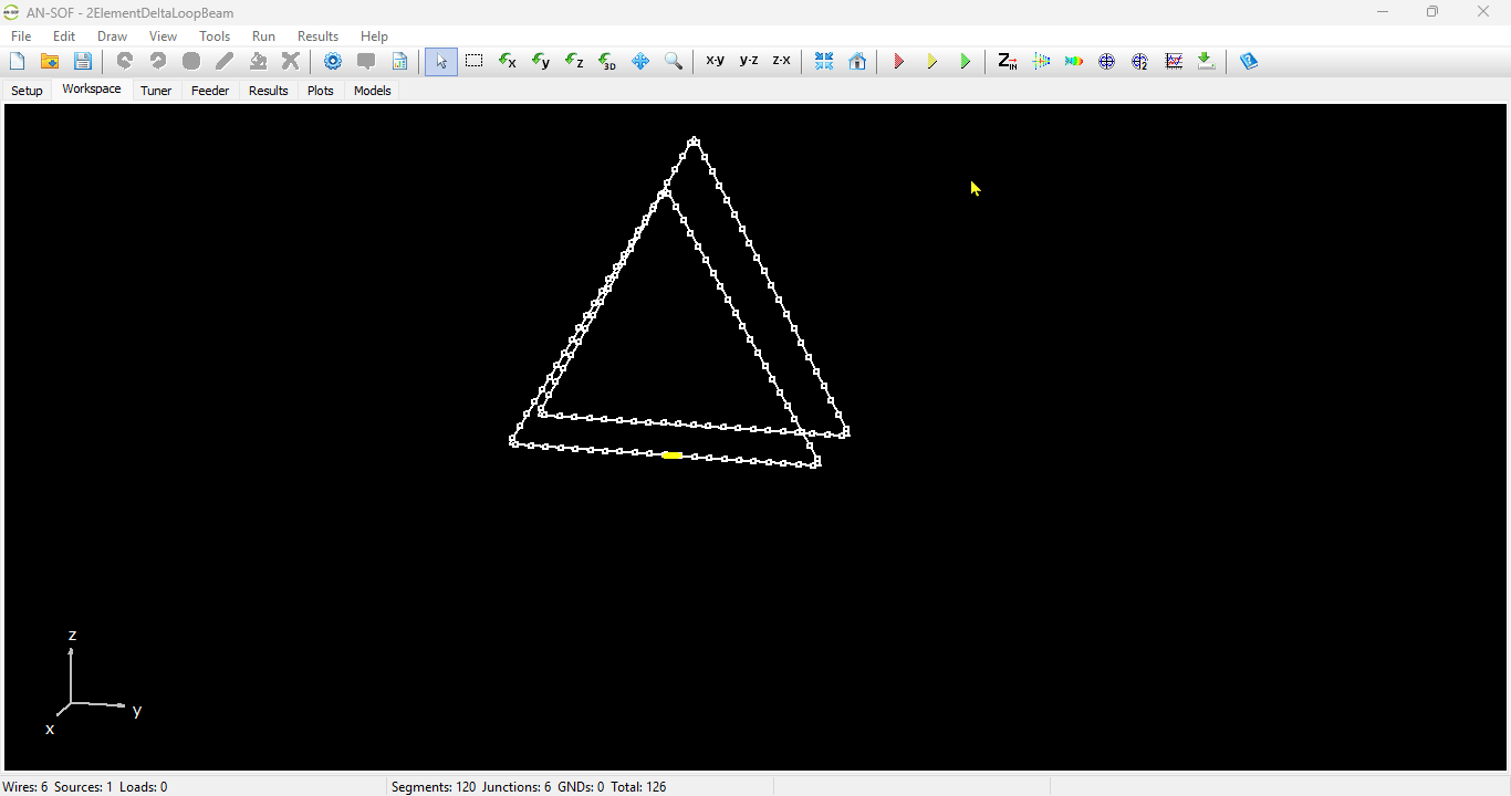
The currents flowing on a wire can be exported to a CSV (Comma-Separated Values) file. Since the current is calculated at the midpoint of each wire segment, the current distribution is sampled at a finite set of points determined by the number of segments the wire is divided into. Additionally, as the current varies with frequency, there is a unique current distribution along the wire for each frequency.
To export the current distribution as a function of position along a selected wire and as a function of frequency, follow these steps:
- Click the Select Wire button (arrow icon) in the toolbar.
- Left-click on the wire to select it (it will be highlighted in light blue).
- Navigate to the Results menu > Export Currents in the main menu (see Fig. 1).
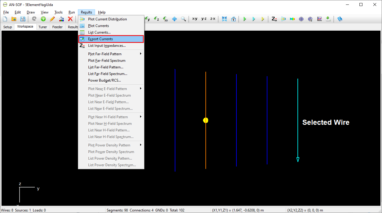
The complex current (real and imaginary parts) is tabulated based on the position along the wire. Position and frequency units can be configured in the Preferences window.
Note:
- Position is measured from the start point of the selected wire (the end without the arrow when selected).
- The exported CSV file contains the real and imaginary parts of the current as a function of position and frequency, as shown in Fig. 2.
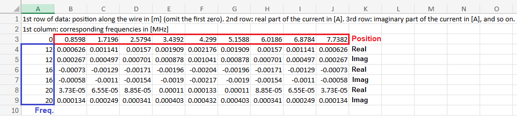
Input Impedances
To analyze the impedance matching and power efficiency of your antenna across the simulated frequency range, use the following procedure:
- Select the Source Wire: Right-click on the wire containing the source to open the pop-up menu.
- Activate the Toolbar: Click the List Currents command to bring up the List Currents toolbar (Fig. 1).
- Target the Source Segment: Use the slider to select the specific segment where the source is located. If you positioned the source at the exact center, the 50% button will jump there instantly.
- Access the Input List: Click the Input List button. This opens the Input List dialog box containing:
- Input Impedance: Real and imaginary parts.
- Source Data: Input current, voltage, and power.
- Matching Parameters: Reflection coefficient, VSWR, and $S_{11}$ (Return Loss) in decibels.
- Visualize the Data:
- XY Plot: Select a parameter (like VSWR or $S_{11}$) from the list in the upper right corner and press Plot to see its frequency response.
- Smith Chart: Press the Smith button to visualize how the input impedance moves across the complex plane relative to the characteristic impedance.
Tips
To ensure your reflection data (VSWR, $S_{11}$, and Return Loss) is accurate for your specific system, you can customize the reference parameters and use shortcuts for single-source models.
Setting the Reference Impedance
By default, calculations are often referenced to $50\ \Omega$, but you can adjust this to match your specific feedline or connector:
- Navigate to the Setup tab in the main workspace.
- Locate the Settings panel.
- Enter your desired value in the VSWR Ref. Impedance field.
Quick Access for Single-Source Models
If your antenna has only one source, you can bypass the segment selection slider and access the input data directly:
- Main Menu: Go to Results > List Input Impedances.
- Toolbar: Click the List Input Impedances icon (ZIN).
The Tuner Calculator
AN-SOF features a tuner calculator that enables impedance matching of an antenna input impedance, an antenna with a feeder already connected to its terminals, or a given custom load.
To access the tuner calculator, choose the Tuner tab in the AN-SOF main window (Fig. 1). Here, you can set the tuner parameters on the left side of the window and view the results on the right side. The tuner consists of three components, each of which will be described in the following sections:
- Impedance Matching Network: This component allows the synthesis of an impedance matching network based on the impedance seen at the network output and the desired impedance at the network input. The quality factors of the network, inductors, and capacitors can be adjusted to model real-world scenarios.
- Stray Capacitance: Some networks, particularly high-pass Tee networks, exhibit a parallel stray capacitance at the network output. This capacitance can be specified to account for this effect.
- Impedance Transformer: An impedance transformer can be specified at the network output to transform the input impedance of an antenna, the input impedance of a feeder connected to an antenna, or a custom load entered by the user. It can represent devices such as baluns and ununs — for example, a 1:1 balun for balanced-to-unbalanced conversion without impedance change, a 1:4 balun to match a 200-ohm antenna to a 50-ohm feedline, or a 1:9 unun for matching high-impedance long-wire antennas. This feature is useful for optimizing power transfer and minimizing VSWR in multiband and off-resonance antenna configurations.
Impedance Matching Network
In the Tuner Parameters box, you can configure the impedance matching network, as shown in Fig. 2.
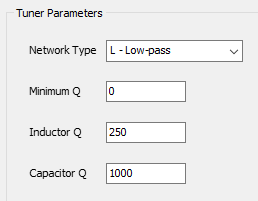
By expanding the Network Type dropdown menu, you have the following options:
- No Network: Select this option to bypass the matching network, making the network input impedance equal to the impedance at the network output.
- Based on the impedance seen at the network output and the source impedance connected to the network input side, AN-SOF can synthesize the following networks:
- L – Low-pass
- L – High-pass
- PI – Low-pass
- PI – High-pass
- T – Low-pass
- T – High-pass
The network components will be automatically calculated to match the source impedance (Rs + jXs) connected to the network input side. If the source impedance has a reactance component, jXs, the network will “absorb” this reactance so that the input impedance of the network plus jXs will match the real part, Rs, of the source impedance. The same principle applies to the load impedance seen at the network output side. If the network load impedance has an imaginary part, it will be absorbed by the network to synthesize the network components (inductors and capacitors).
Note that a low-pass network could include series capacitors instead of inductors or parallel inductors instead of capacitors, depending on the complex impedances (with real and imaginary parts) being matched. Similarly, a high-pass network might involve series inductors instead of capacitors or parallel capacitors instead of inductors.
You can specify a minimum Q for the network synthesis calculations, as well as the Q for the inductors and capacitors. This allows you to account for component losses to represent real-world components. To model ideal zero-loss components, enter high Q values, such as 1E8.
Stray Capacitance
Stray capacitance, also known as parasitic capacitance, refers to unintended capacitance between two conductors separated by a dielectric or free space. This effect is particularly noticeable at the network output side when a transmission line is connected. AN-SOF allows for the configuration of a feeder composed of a transmission line to feed an antenna, enabling modeling of stray capacitance to accommodate this scenario. While stray capacitance is commonly observed in Tee high-pass networks, it can be added in any case. Typical values range from around 10 pF in HF bands.
Impedance Transformer
In the Tuner Parameters box, an impedance transformer, also known as a “trafo” in RF jargon, can be specified, as shown in Fig. 3.
The transformer allows us to divide a load impedance by a factor, n, making it a 1:n transformer. It’s important to note that this is the impedance transformation factor, not the voltage transformation factor, which is n-1/2 and is determined by the primary-to-secondary winding relationship of a transformer. A transformer can be used to reduce a high impedance to approach the standard 50 or 75 Ohms used in transmission lines and RF devices. Both the real and imaginary parts of the load impedance will be divided by n.
If n is in the range 0 < n < 1, the transformed impedance will be higher than the load impedance connected to the output side of the transformer. A factor n = 1 can be used to model a 1:1 transformer, also known as an isolation transformer, which is used to transfer voltage from one electrical circuit to another and to isolate a powered device from the power source. The 1:1 ratio transformer has the same input and output voltage and current. It is used to protect secondary circuits and individuals from electrical shocks between energized conductors and earth ground. It also reduces voltage spikes in the power supply line caused by rapid changes in lighting, static electricity, or voltage.
Real-life transformers are manufactured for a specified nominal impedance transformation. The nominal impedance can be entered in the Tuner Transformer box, as well as the transformer insertion loss in decibels. Manufacturers specify a transformer insertion loss relative to a nominal impedance, so it is important to specify the nominal impedance as well. The insertion loss is defined as the power lost inside the transformer, measured in dB relative to the input power. Thus, the output power delivered by the transformer to the load impedance will be lower than the input power due to losses inside the transformer materials (coil conductor losses, magnetic core losses, etc.).
Tuner Frequency and Input Power
The components synthesized in the impedance matching network of the tuner will be automatically calculated for a specified frequency, which can be chosen from a dropdown menu in the Tuner Parameters box, as shown in Fig. 4.
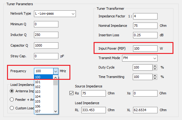
This list of frequencies is taken from the Frequency panel in the Setup tab, where a single frequency, a list of frequencies, or a frequency sweep can be configured. Therefore, to change the list of frequencies available in the Tuner tab, go to the Setup tab and enter the desired frequencies in the Frequency panel. Note that the frequency chosen for the tuner will be its design frequency; thus, the tuner components, inductors, and capacitors will be recalculated if the design frequency changes.
The Input Power to the tuner can also be specified in the Tuner Parameters box. This is the power delivered by the source connected to the input side of the impedance matching network of the tuner. This input power affects the powers calculated in the Results box on the right side of the Tuner tab, as explained below. It is worth mentioning that the tuner input power is not the power delivered to the antenna terminals, which can be set in the Excitation panel of the Setup tab. However, if the tuner is connected to an antenna, we can specify that the tuner output power be delivered to the antenna terminals, as detailed below.
Transmit Mode, Duty Cycle, and Time Transmitting
The input power specified is the transmitter’s Peak Envelope Power (PEP). However, when performing RF exposure evaluations, the average power supplied by the transmitter over time is the critical factor. The average power is a fraction of the PEP, determined by the duty cycle (or duty factor) of the selected transmit mode. The transmit mode can be chosen, and the corresponding percentage duty cycle will be displayed, as shown in Fig. 5. To enter a custom duty cycle, select “Custom” as the transmit mode.
It is also important to account for the percentage of time the transmitter remains active within a specific period, such as 6 minutes. For example, if the telegraph mode transmits for only 3 minutes in every 6-minute period, the power considered for RF exposure calculations is reduced by 50%. Therefore, the Time Transmitting parameter can be set as a percentage. Both the duty cycle and the time transmitting percentage will affect the PEP, and an average input power will be calculated accordingly.
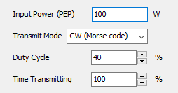
Tuner Source and Load Impedances
The source impedance connected to the tuner input side can be set in real (Rs) and imaginary (Xs) parts, as shown in Fig. 6.
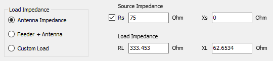
When a non-null source reactance, Xs, is entered, it will be absorbed by the impedance matching network calculations. Thus, the net input impedance of the network, after adding jXs, will be matched to the real part of the source impedance, Rs. Click on the checkbox next to the “Rs” label to set this resistance as the reference impedance for VSWR calculations. This same resistance will be automatically set in the Settings panel as the “VSWR Ref. Impedance”.
There are three options for the tuner load impedance (RL + jXL):
- Antenna Impedance: Select this option to set the antenna input impedance as the tuner load. Note that the antenna impedance varies with frequency, so changing the design frequency for the tuner will trigger a recalculation of the impedance matching network.
- Feeder + Antenna: This option allows us to set the combination of feeder + antenna as the tuner load. In this case, the feeder parameters will be taken from the Feeder tab at the chosen design frequency. Therefore, the load impedance connected at the tuner output is a function of frequency since it is the input impedance to the feeder connected to the antenna.
- Custom Load: This option allows setting a tuner load impedance manually by specifying its real (RL) and imaginary (XL) parts. The Tuner tab can be used as an independent impedance matching calculator in this case.
Tuner Results
The results of the calculations based on the configured tuner parameters are displayed in the Results box on the right side of the Tuner tab, as shown in Fig. 7.
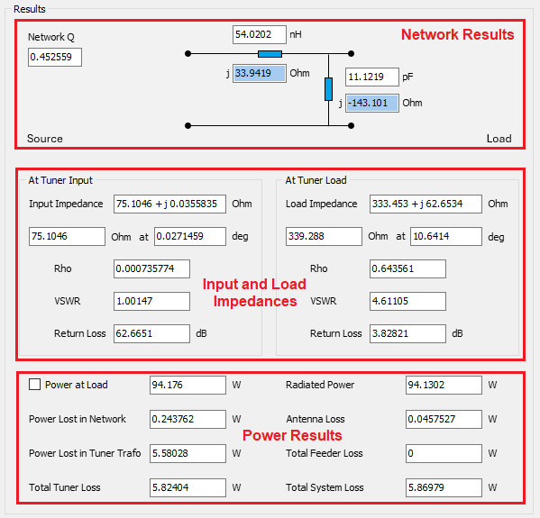
The results are categorized into three sections: Network results, input and load impedances, and power results.
Network Results
The network results shown include the resulting network Q and a diagram illustrating the network components, including inductors and capacitors. For inductors, their inductance in Henry and reactance in Ohms will be displayed, while for capacitors, their capacitance in Farads and reactance in Ohms will be shown. The units of inductance and capacitance displayed can be changed to pH, nH, uH, mH, H, or pF, nF, uF, mF, F, respectively, by navigating to the AN-SOF main menu > Tools > Preferences > Units tab.
It’s worth mentioning that the resulting network Q for L-type networks is determined only by the impedances connected to the load and source side of the network. Therefore, the minimum Q specified in the Tuner Parameters box has no effect for L networks.
Tuner Input and Load Impedances
The resulting input impedance to the tuner will be displayed in both real and imaginary parts, along with a polar representation showing its magnitude in Ohms and phase in degrees. If the source impedance, Rs + jXs, connected to the tuner has a non-null reactance, jXs, this will be absorbed by the impedance matching network. Consequently, the displayed tuner input impedance represents the impedance seen towards the tuner just after Rs, as illustrated in the diagram on the left side of the Tuner tab (Fig. 8).
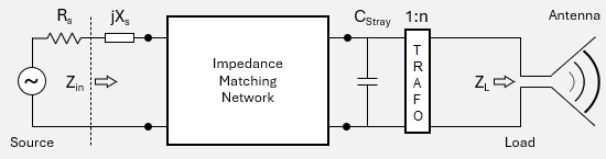
The load impedance connected to the tuner output terminals will also be shown, which can be the antenna input impedance, a feeder + antenna combination, or a user-entered impedance in the Tuner Parameters box on the left side of the Tuner tab.
For both the tuner input and load impedances, the reflection coefficient (Rho), VSWR, and return loss in dB will be displayed. These values are referred to the reference impedance for VSWR, which has been configured in the Settings panel of the Setup tab.
Powers Delivered and Lost
At the bottom of the Results box, the following powers are calculated:
- Power at Load: This is the power effectively delivered to the tuner load impedance. Note that the tuner consists of the impedance matching network + stray capacitance + transformer sequence. Therefore, the power at the tuner load represents the power delivered at the transformer output terminals. If an antenna impedance is chosen as the tuner load, the “Power at Load” is the power delivered to the antenna terminals. If a feeder + antenna is chosen as the tuner load, the “Power at Load” is the power delivered to the feeder terminals. To apply this power to the antenna model in the Workspace tab, check the checkbox next to the “Power at Load” label.
- Power Lost in Network: This is the total power lost in the network components, including inductors and capacitors, due to the losses related to the specified quality factors, Q. In the impedance matching network, a resistance, R = X/Q, representing component losses, is added in series to the inductor and capacitor reactance, X.
- Power Lost in Tuner Trafo: This is the power lost in the impedance transformer due to the specified insertion loss.
- Total Tuner Loss: This is the sum of the network and transformer losses.
- Radiated Power: If an antenna impedance is set as the tuner load, this is the power effectively radiated by the antenna after discounting losses in the antenna system. If a feeder + antenna is set as the tuner load, this is the power radiated by the antenna after discounting losses in the feeder and the antenna system.
- Antenna Loss: This is the power lost in the antenna structure, considering conductor losses, transmission line losses, if any, and ground plane losses.
- Total Feeder Loss: If a feeder + antenna is chosen as the tuner load, this is the power lost in the feeder system.
- Total System Loss: This is the sum of the power lost in the tuner (network + transformer), antenna (conductors, transmission lines, and ground plane), and feeder (feeding line + transformer), if specified.
The Smith Chart is an essential tool for visualizing the input impedance of your antenna as it varies with frequency. It allows you to see how “matched” your antenna is to a reference system (typically $50\ \Omega$) at a glance.
How to Generate the Chart
- Follow the procedure for Listing the Input Impedances: Right-click source wire > List Currents > Input List (Fig. 1).
- In the Input List dialog box, click the Smith button. This launches the AN-Smith application.
Interactive Features in AN-Smith
- Data Hints: Left-click anywhere on the impedance curve. A hint message will appear displaying the Frequency, Input Impedance (Zin), Reflection Coefficient (Rho), VSWR, and S11 for that specific point.
- Admittance Plotting: To switch from impedance coordinates to admittance, go to the main menu and select Plot > Admittance.
- Customization: Navigate to Edit > Preferences to adjust the visual appearance, such as line thickness and colors.
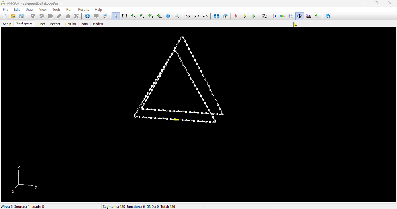
Antenna Feeder Calculator
In this article, you will learn how to add a feed line and transformer to your AN-SOF project. These components are essential for connecting your antenna structure to the external circuitry and impedance matching.
In the case of a transmitting antenna with a single feed port, the feeder used to connect the transmitter to the antenna terminals can be modeled in the Feeder tab, as shown in Fig. 1. The feeder consists of a transmission line, or feed line, and an impedance transformer.
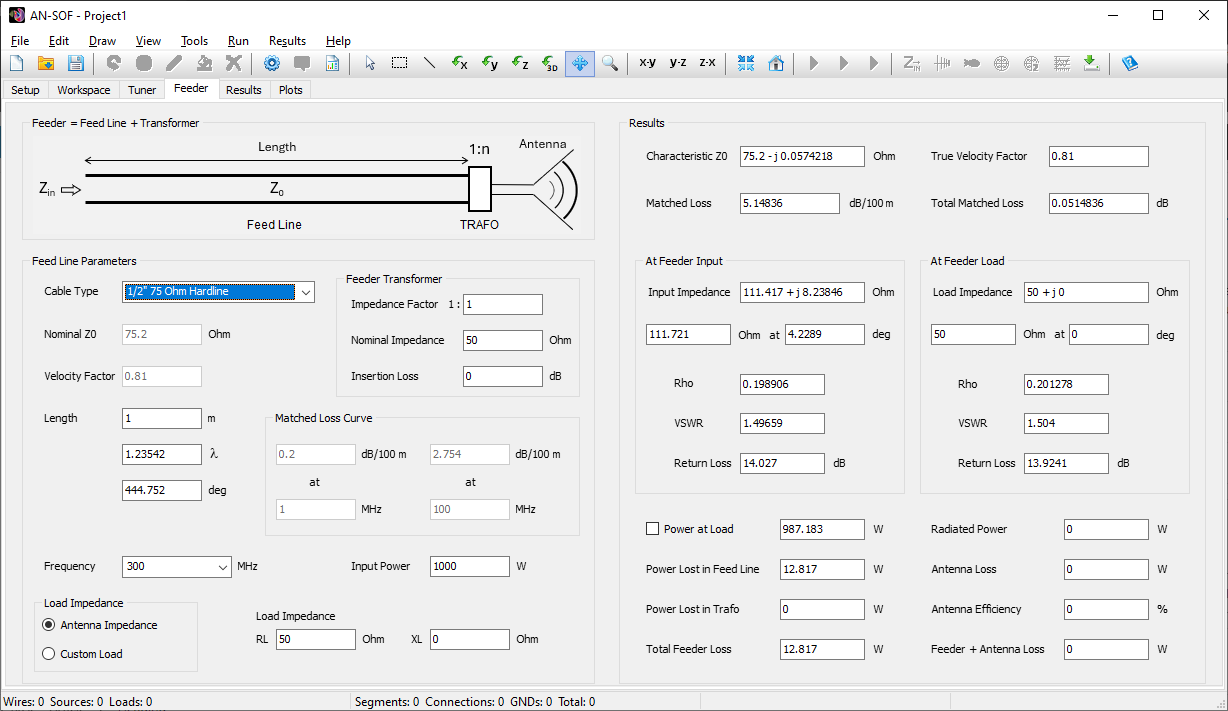
Setting the Impedance Transformer
The transformer, also known as trafo, can represent a balun or unun that connects directly to the antenna terminals to divide its input impedance by a factor, n. In the Feeder Transformer box, three parameters can be specified:
Impedance Factor 1:n
Here, “n” is the factor by which the antenna input impedance will be divided. For example, if we have a folded half-wave dipole, which typically has an input impedance on the order of 300 Ohms, we can set n = 4 to get 300/4 = 75 Ohms of input impedance after the transformer (i.e., a 1:4 balun). If the input impedance is complex, both its real and imaginary parts will be divided by n.
If the transformation factor is in the range 0 < n < 1, the transformer input impedance will be greater than the antenna impedance. By setting n = 1, we can represent a 1:1 transformer, also known as a common-mode choke or line isolator, used to transform a balanced or symmetrical antenna to an unbalanced feed line.
Note that “n” is the impedance transformer factor, not the voltage transformation factor. In a transformer, which is composed of a primary winding (inductor or coil) and a secondary winding, the voltage transformation factor is n-1/2.
Nominal Impedance
All actual impedance transformers, whether baluns or ununs, are fabricated for a nominal impedance, for which the manufacturer warranties the transformer performance in terms of bandwidth and insertion loss. So, if a lossy transformer is going to be modeled, we should set its nominal impedance according to the manufacturer’s datasheet.
Insertion Loss
The insertion loss of the transformer can be set in decibels to represent the actual loss given in its datasheet. The insertion loss is defined as the power lost, in decibels, inside the transformer, so that its output power will be lower than its input power due to losses in the transformer materials (coil resistivity, magnetic core losses, etc.).
Note: If no transformer is needed, just set n = 1 and an insertion loss of 0 dB.
Setting Feed Line Parameters
In AN-SOF, various real-life transmission line types are available, each with matched loss parameters adjusted according to the cable datasheets. These cable types are organized by part numbers and include the manufacturer’s name.
For example, entering “RG-8” in the Cable Type option will display this part number for different manufacturers, as shown in Fig. 2. Selecting RG-8 Belden 8237 will reveal a set of K0, K1, and K2 parameters. These constants have been adjusted to match the loss curve as a function of frequency, based on the matched loss vs. frequency table published in the cable datasheet. K0 relates to the DC losses in the transmission line conductors, K1 to the skin effect losses dependent on the square root of frequency, and K2 to dielectric losses increasing linearly with frequency. These losses are then considered in the standard RLGC model of a lossy transmission line.
The nominal values of the cable characteristic impedance Z0 and velocity factor will also be shown for the chosen part number and manufacturer. After selecting the cable type, you can set the operating frequency and input power to the feed line. The frequency can be chosen from a list that displays the frequencies set in the Setup tab.
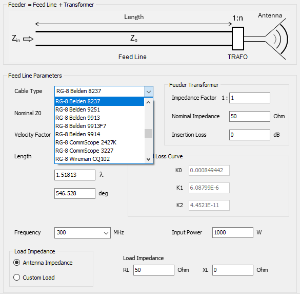
Next, you can set the length of the cable, entered according to the length unit used for drawing wires in the workspace. To change the length unit, go to Tools > Preferences in the main menu. As you type the cable length, the length measured in wavelengths (λ) and electrical degrees will be automatically displayed. In fact, all feed line results are calculated automatically by modifying any of the feed line parameters.
You can then choose the load impedance of the feed line. The default option considers the Antenna Impedance as the load impedance of the transmission line, automatically displaying the antenna input impedance at the chosen frequency as the load for the line. However, you can enter any value for the line load impedance by selecting the Custom Load option. This allows you to use the Feed Line tabsheet as an independent calculator for transmission lines.
After specifying the feeder parameters in the left side of the Feeder tab, the following results will be obtained in its right side (Fig. 1):
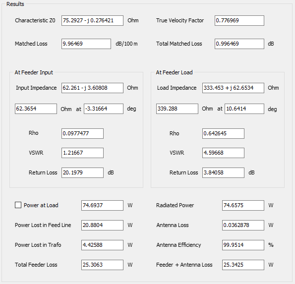
Characteristic Z0
This is the “true” characteristic impedance of the feed line obtained from the RLGC model via the K0, K1, and K2 constants. The real part of Z0 may differ somewhat from the nominal Z0 depending on frequency and losses in the transmission line. An imaginary part will always appear in Z0 due to non-zero losses. So, note that the true characteristic Z0 will generally differ from the “Nominal Z0” (Z0 in the cable datasheet).
True Velocity Factor
This is the “true” velocity factor obtained from the RLGC model of the transmission line, where the wavenumber (and wavelength inside the line) is affected by losses. The velocity factor will be modified relative to its nominal value accordingly. Therefore, the true velocity factor is a function of frequency and losses in the line.
Matched Loss
Any cable datasheet contains a table of matched loss values expressed in dB/100 feet or dB/100 m as a function of frequency. These values correspond to the attenuation of the line when it is matched (the line has a load impedance equal to Z0). So, the Matched Loss value shown in the Results panel is the attenuation of the line corresponding to the selected frequency.
Total Matched Loss
This is the matched loss that would be obtained for the specified length of the cable. Therefore, the Total Matched Loss equals the Matched Loss (dB/100 feet or dB/100 m) multiplied by the cable length.
At Feeder Input
The input impedance of the feeder (feed line + transformer) will be shown as well as the reflection coefficient (Rho), VSWR, and return loss, all referred to the true characteristic impedance of the feed line. This is the impedance at the feed line end opposite to the end where the load or antenna is connected.
At Feeder Load
The load impedance connected to the feeder (feed line + transformer) will be shown as well as the reflection coefficient (Rho), VSWR, and return loss, all referred to the true characteristic impedance of the feed line. The load impedance will be the antenna input impedance if the Antenna Impedance option was selected as a parameter for the feed line in the left side of the Feeder tab. If a “Custom Load” was selected, then the load impedance will be that entered by the user.
Power at Load
This is the power in Watts consumed at the feeder load impedance or effectively delivered to the antenna terminals. This power will be less than the input power specified as an input parameter for the feed line if the transmission line has losses. The power at the load will be equal to the input power in the case of a lossless transmission line. Check the Power at Load option to automatically set this power as the input power delivered to the antenna terminals. Otherwise, the antenna input power will be that set manually in the Excitation panel of the Setup tab.
Power Lost in Feed Line
This is the power lost along the transmission line in Watts.
Power Lost in Trafo
This is the power lost in the feeder transformer in Watts.
Total Feeder Loss
This is the sum of the powers lost in the feed line and in the transformer.
Radiated Power
This is the power in Watts radiated by the antenna when it is fed using the Power at Load, which is the power effectively delivered to the load impedance of the feeder. The radiated power will be different from the power delivered by the feeder if the antenna itself has its own losses. The radiated power will be shown if the option Antenna Impedance was selected as a load impedance for the feeder in the left side of the Feeder tab.
Antenna Loss
This is the power lost in the antenna structure. It will be shown if the option Antenna Impedance was selected as a load impedance for the feeder in the left side of the Feeder tab.
Antenna Efficiency
This is the ratio of the antenna radiated power to the antenna input power (the power delivered by the feeder). It is expressed as a percentage as it is usual. It will be shown if the option Antenna Impedance was selected as a load impedance for the feeder in the left side of the Feeder tab.
Feeder + Antenna Loss
This is the sum of the powers lost in the feeder (feed line + transformer) and antenna.
In addition to the manufactured cables listed in the Cable Type option, the following custom line options can be chosen, as shown in Fig. 1:
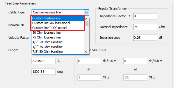
Custom lossless line
This option represents an ideal transmission line with zero losses. Only the nominal Z0 and velocity factor can be specified in this case.
Custom line low-loss model
This option allows the specification of the nominal Z0, velocity factor, and matched loss curve. To define the matched loss curve, two values of attenuation must be entered at two different frequencies, with the second frequency being greater than the first one. AN-SOF will adjust a low-loss model to obtain a curve of attenuation vs. frequency for subsequent calculations. While the real part of the characteristic Z0 will be equal to the nominal Z0 in the low-loss model, which is a good approximation in many cases, especially for higher frequencies, the characteristic impedance will have an imaginary part that depends on the line losses and frequency. The “true” velocity factor is also assumed to be equal to the nominal velocity factor.
Custom line RLGC model
This option represents a transmission line model where losses are accurately considered by adjusting a matched loss curve to the table of attenuation vs. frequency in the cable datasheet. The K0, K1, and K2 constants must be entered in this case. The definition of K0, K1, and K2 considers that the frequency is in Hz and lengths are in meters (SI metric units). This option allows the entry of K0, K1, and K2 obtained from other transmission line calculators.
Load Impedances
Analyzing how power is dissipated or transferred through lumped loads (such as resistors, inductors, or capacitors) is vital for understanding matching networks or loaded antenna performance. Use the following steps to tabulate and plot these values:
- Select the Loaded Wire: Right-click on the wire where you have placed a load to open the pop-up menu.
- Open the “List Currents” Toolbar: Select the List Currents command (Fig. 1).
- Navigate to the Load: Use the slider to move to the specific segment containing the load.
- Access the Load List: Click the Load List button (this button remains disabled unless a load is detected on the selected segment).
Data Interpretation and Plotting
The Load List dialog box provides a detailed breakdown of the following parameters across your frequency range:
- Load Current and Voltage: The actual values present at the load’s terminals.
- Power: The real and reactive power consumed by the load.
- Impedance: The calculated impedance of the load at each frequency step.
To visualize this data, select the desired parameter from the menu in the upper-right corner and click the Plot button to open the AN-XY Chart.
In many simulations, a source isn’t just an ideal voltage; it often includes an internal impedance that accounts for the physical characteristics of the feedline or generator. You can analyze how much power is lost internally versus how much is delivered to the antenna by following these steps:
- Locate the Source: Right-click on the wire where the source is positioned to open the pop-up menu.
- Open the “List Currents” Toolbar: Select List Currents to activate the corresponding toolbar.
- Select the Source Segment: Use the slider (or the 50% button if centered) to highlight the segment containing the source.
- Open the Source List: Click the Source List button. This opens a dialog box that focuses specifically on the internal behavior of the source (Fig. 1).
Evaluating Internal Parameters
The Source List dialog provides a frequency-by-frequency breakdown of:
- Internal Current & Voltage: The electrical values specifically across the source’s internal impedance.
- Internal Power: Useful for determining if the generator is properly matched to the load (the antenna).
To visualize these trends, select an item from the list in the upper-right corner and click Plot to view it in AN-XY Chart.
Far Field
Rectangular Plots
The radiation pattern can be visualized as a 2D rectangular plot by navigating to Results > Plot Far-Field Pattern > 2D Rectangular Plot from the main menu. This action opens the Radiation Pattern Cut dialog box (Fig. 1), which offers two primary cut types:
- Conical Plots: Generated with a fixed $\theta$ (Theta, zenith) and variable $\phi$ (Phi, azimuth).
- Vertical Plots: Created with a fixed $\phi$ (Phi, azimuth) and variable $\theta$ (Theta, zenith).
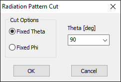
Upon selecting a cut and clicking OK, the AN-XY Chart application (Fig. 2) is launched. The pattern is plotted against Phi for conical cuts or against Theta for vertical cuts.
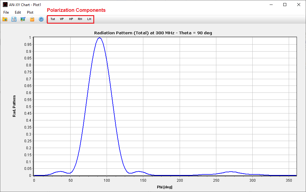
Parameter Visualization and Polarization
Within the AN-XY Chart application, the Plot menu allows you to graph a comprehensive suite of parameters, including:
- Metrics: Power Density, Directivity, Gain, E-field, and Axial Ratio.
- Units: Data can be represented in linear units or decibels (e.g., dBi for directivity and gain).
- Polarization Decomposition: Metrics can be decomposed into:
- Linear Components: Theta (VP: Vertically Polarized) and Phi (HP: Horizontally Polarized).
- Circular Components: Right (RHCP) and Left (LHCP).
The toolbar provides rapid-access buttons (Tot, VP, HP, RH, LH) to switch between the total field and its polarized components, facilitating a detailed analysis of the antenna’s polarization purity.
Receiving and Scattering Modes (RCS)
When using plane wave excitation, where the antenna is in receiving mode or a metallic structure is scattering waves, the software automatically plots the Radar Cross Section (RCS) instead of directivity or gain. This scattered field pattern is observed in the far-field region, where the scattered field amplitude decays at a rate of $1/r$ and the power density follows the inverse square law ($1/r^2$).
The Axial Ratio
The Axial Ratio is defined as the ratio of the minor axis to the major axis of the polarization ellipse.
- Range: It ranges from 0 to 1 in absolute value (also plottable in dB).
- Circular Polarization: Indicated by an axial ratio of $\pm 1$ (or 0 dB).
- Linear Polarization: Indicated by an axial ratio of zero.
- Sense: A positive value indicates right-handed polarization, while a negative value indicates left-handed polarization.
Polar Plots
For a classic representation of antenna performance, the far-field pattern can be visualized in a 2D polar chart by selecting Results > Plot Far-Field Pattern > Polar Plot 1 Slice from the AN-SOF main menu (Fig. 3). This action launches the AN-Polar application, a dedicated environment for analyzing directional characteristics.
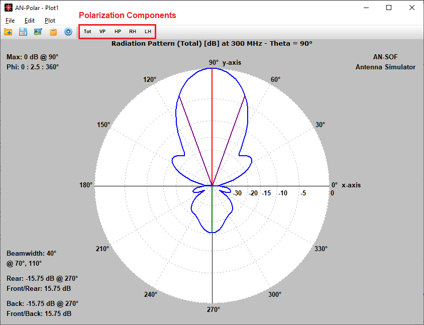
Polarization and Multi-Slice Analysis
The AN-Polar interface includes a specialized toolbar with buttons (Tot, VP, HP, RH, LH) that allow for the immediate decomposition of the pattern into its respective linear or circular polarization components.
To compare different planes of radiation simultaneously:
- Navigate to Results > Plot Far-Field Pattern > Polar Plot 2 Slices.
- Use the resulting dialog box (Fig. 4) to overlay two distinct slices on a single chart.
- Available combinations include two vertical slices (E and H planes), two conical slices, or a vertical-conical hybrid view.
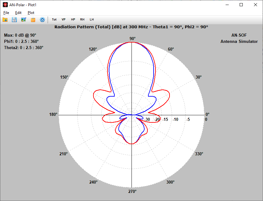
Interactive Metrics and Auto-Calculation
AN-Polar provides real-time data feedback. Clicking any point on the polar curve displays the specific metric value and its associated polar angle. When a single slice is plotted, the software automatically calculates and displays key performance metrics in the lower-left corner:
- Beamwidth: The angular width between the -3 dB points.
- Front-to-Back (F/B) Ratio: The ratio of power in the primary lobe to that at exactly 180°.
- Front-to-Rear (F/R) Ratio: The ratio of the main lobe to the maximum level in the entire rear hemisphere (worst-case scenario).
See Also:
Customization and Scaling (AN-Polar Preferences)
The Preferences window (Fig. 5), accessible via the Edit menu or the gear icon, allows for deep customization of the visual output, including title editing, line thickness, font selection, and plot rotation.
A critical feature within this window is the Scale Type selection:
- Linear (Lin): A standard “textbook” scale where radial distances are divided into equal intervals.
- Logarithmic (Log): An “ARRL-style” log scale. This scale follows the traditional standards used in ARRL publications and handbooks. It is particularly advantageous for antenna designers as it expands the visualization of small secondary lobes and nulls that are often compressed and difficult to resolve in a linear scale.

The far-field distribution can be visualized as a comprehensive 3D plot by selecting Results > Plot Far-Field Pattern > 3D Plot from the AN-SOF main menu. This command launches the AN-3D Pattern application, which renders the radiation pattern in a three-dimensional space, using a dynamic color scale to represent field intensities across the lobes.
Field Metrics and Polarization Decomposition
The Plot menu within AN-3D Pattern provides access to a wide array of electromagnetic metrics (Fig. 1), including:
- Power Density and E-field
- Directivity and Gain: Available in both numerical (linear) and dBi scales.
- Radiation Pattern: Normalized to unity (1.0) or 0 dB.
- Axial Ratio: Presented as a dimensionless value or in dB.
Each metric can be decomposed into its constituent polarization components using the toolbar buttons (Tot, VP, HP, RH, LH). This allows for the isolated analysis of:
- Linear Polarizations: $\theta$ (Theta, Vertical) and $\phi$ (Phi, Horizontal).
- Circular Polarizations: Right-Handed (RHCP) and Left-Handed (LHCP).
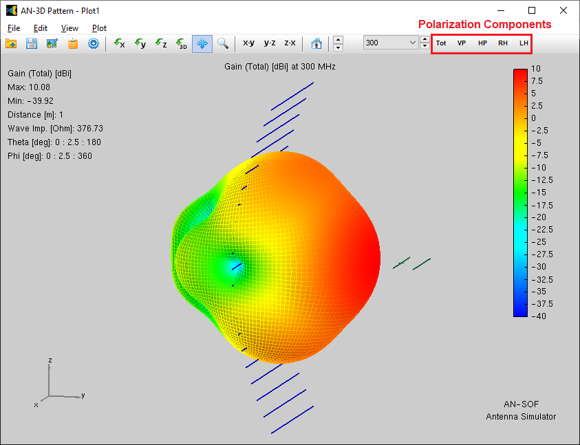
Radar Cross Section (RCS)
For simulations involving plane wave excitation (such as scattering analysis or an antenna in receiving mode), the software enables the plotting of the Radar Cross Section (RCS). The resulting 3D visualization represents the scattered field pattern as observed in the far-field region, where field amplitude decays by $1/r$ and power density by $1/r^2$.
Analyzing the Axial Ratio
The 3D Axial Ratio pattern illustrates the ratio between the minor and major axes of the polarization ellipse.
- Linear Polarization: Indicated by a value of 0.
- Circular Polarization: Indicated by a value of 1.
While the 3D plot excels at showing the magnitude of the axial ratio, the sign (which defines the sense of rotation as RHCP or LHCP) is best verified in a 2D rectangular plot. However, the rapid-switching polarization buttons on the 3D toolbar, RH and LH, provide an efficient alternative for identifying dominant polarization handedness.
Navigation and Dynamic Frequency Sweeping
The 3D environment is fully interactive, allowing for detailed inspection of the radiation structure:
- Manipulation: Use the 3D Rotation or Move buttons on the toolbar to rotate or translate the view by clicking and dragging. Zooming is handled via the mouse wheel.
- Dynamic Frequency Sweep: A key feature of the AN-3D Pattern toolbar is the ability to toggle the operating frequency. By using the up-down arrow buttons next to the frequency display, users can observe the radiation lobes evolve dynamically, effectively creating an animation of the antenna’s wideband performance.
3D Visualization and Data Management in AN-3D Pattern
To access the Preferences dialog box in the AN-3D Pattern application, navigate to Edit > Preferences in the main menu (Fig. 2). This interface allows for deep customization of the 3D visualization, including the appearance of the colored surface and the density of the mesh overlay on the radiation lobes (Fig. 3).
For enhanced spatial context, you can superimpose the physical wire structure onto the radiation pattern by checking the Wires option within the “Show” panel. This panel also provides controls for the graph’s scale and the toggle for displaying the coordinate axes ($x, y, z$).
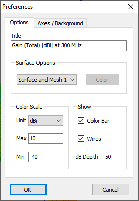
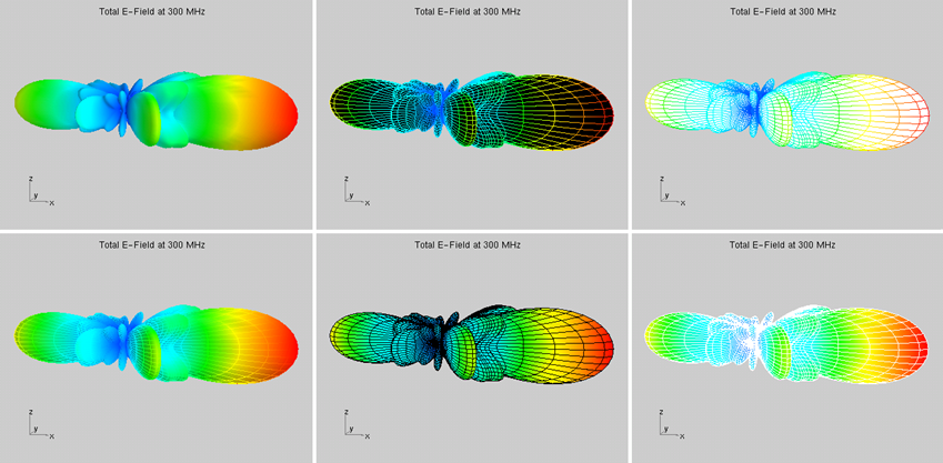
Data Export and Tabulation
While the 3D graphical representation is intended for visualization, the raw far-field data for a specific frequency can be extracted by returning to the AN-SOF main menu. Select Results > List Far-Field Pattern to generate a tabular view of the results. From there, click the Export button to save the dataset as a CSV (Comma Separated Values) file, which can be imported into external spreadsheet or analysis software.
Note
- If discrete sources were used as the excitation of the structure, the plotted far-field represents the total field.
- If an incident plane wave was used as the excitation, the plotted far-field represents the scattered field.
Far-field frequency spectra are generated when a simulation is executed using a specified list of frequencies or a frequency sweep. At each frequency point, the far field is calculated over the angular range (Theta and Phi) and observation distance defined in the Field panel of the Setup tab. To visualize the far field as a function of frequency, a fixed observation direction, defined by specific Zenith (Theta) and Azimuth (Phi) angles, must be selected.
Generating the Spectrum Plot
To visualize the spectrum, navigate to Results > Plot Far-Field Spectrum in the main menu. This action opens the Select Far-Field Point dialog box (Fig. 1), where the target Theta and Phi coordinates are specified. Upon clicking OK, the AN-XY Chart application displays the far-field spectrum relative to frequency (Fig. 2).
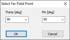
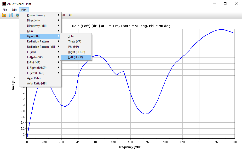
Available Metrics and Polarization Analysis
The Plot menu in the AN-XY Chart application provides access to several critical far-field metrics, including:
- Power Density, Directivity, and Gain.
- Radiation Pattern and E-Field.
- Axial Ratio.
Most metrics can be toggled between linear units and decibels. Furthermore, the software supports polarization decomposition into VP (Vertical), HP (Horizontal), RHCP (Right-Hand), and LHCP (Left-Hand) components. The application toolbar allows for rapid switching between these polarization states (Fig. 3).
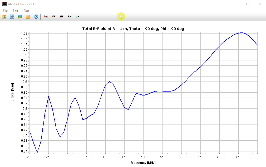
Electric Field Components and Axial Ratio
Users can plot the linearly polarized electric field components ($E_\theta$ and $E_\phi$) or circularly polarized components ($E_{\text{Right}}$ and $E_{\text{Left}}$) against frequency. Each component can be analyzed through:
- Amplitude and Phase.
- Real and Imaginary parts.
The Axial Ratio, representing the ratio of the minor to major axes of the polarization ellipse, is also available as a function of frequency. This is a vital tool for verifying the circular polarization bandwidth of an antenna, plottable in both linear and dB scales.
Tabular Data and Visualization
The far-field spectrum for a selected observation point can also be reviewed in a tabular format. By selecting Results > List Far-Field Spectrum from the main menu and specifying the Theta and Phi coordinates, a table is generated listing all field components versus frequency. From this view, clicking the Plot button provides an alternative route to visual data analysis (Fig. 4). This suite of tools is essential for evaluating the wideband performance and stability of an antenna design.
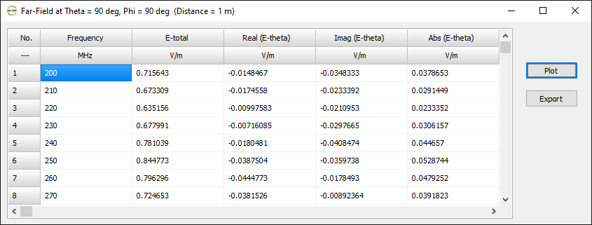
To access the Power Budget dialog box (Fig. 1), navigate to Results > Power & Scattering Metrics in the main menu. When discrete sources are used for excitation, the following list of parameters versus frequency is displayed:
Parameters
- Input Power: Total input power provided by the discrete sources in the structure.
- Radiated Power: Total radiated power from the structure.
- Structure Loss: Total consumed power, representing ohmic losses in the structure.
- Efficiency: Radiated power-to-input power ratio, representing the radiation efficiency. For a lossless structure, this value is 100%.
- Directivity: Peak directivity, displayed both as a dimensionless value and in decibels (dBi) relative to an isotropic source.
- Gain: Peak gain, displayed both as a dimensionless value and in decibels (dBi) relative to an isotropic source.
- Av. EIRP (Effective Isotropic Radiated Power): Time-averaged EIRP in Watts and dBW. This value accounts for the duty cycle of the selected transmit mode in the Tuner tab and the Time Transmitting percentage.
- Peak EIRP (Effective Isotropic Radiated Power): Peak EIRP in Watts and dBW, calculated directly from the Peak Envelope Power (PEP) without considering the duty cycle or time transmitting percentage.
- Av. Power Density: Average power density, calculated by averaging the power density over all directions in space.
- Peak Power Density: Maximum value of the radiated power density.
- Theta (max) and Phi (max): The zenith and azimuth angles, respectively, in the direction of maximum radiation, corresponding to the peak power density.
- F/R H and F/B H: Front-to-rear and front-to-back ratios, respectively, in a horizontal slice of the radiation pattern given by Theta = Theta (max).
- F/R V and F/B V: Front-to-rear and front-to-back ratios, respectively, in a vertical slice of the radiation pattern given by Phi = Phi (max).
Error and Average Gain Test (AGT)
- Error: Represents the error in the power balance of the system. A necessary (but not sufficient) condition for a valid model is that the input power must equal the sum of the radiated and lost powers. The error is calculated as:
$\displaystyle \text{Error %} = 100 \times \frac{\text{Input Power} \,-\, \text{Lost Power} \,-\, \text{Radiated Power}}{\text{Input Power} \,-\, \text{Lost Power}}$
- Average Gain Test (AGT): A validation metric that should be close to 1 for a valid model. It is calculated as:
$\displaystyle \text{AGT} = \frac{\text{Radiated Power} + \text{Lost Power}}{\text{Input Power}}$
Plotting and Exporting Data
- Select an item from the list in the upper-right corner of the window and click the Plot button to plot the selected item versus frequency.
- Click the Export button to export the list to a CSV file.
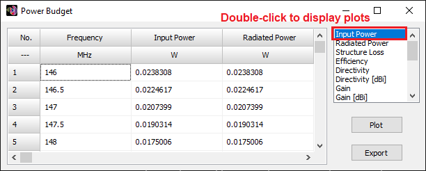
Notes
- A power budget error of about ±10% is permissible from the engineering point of view.
- When a real ground plane is used, the Error column shows the percentage of power lost in the ground due to its finite conductivity.
- When a substrate slab is used, this column shows the percentage of power transferred to the dielectric material in the substrate (surface wave loss).
- AGT = 1 means that the power balance is exact. An AGT between 0.99 and 1.01 is comparable to achieving an error of ±1%.
AN-SOF calculates the bistatic Radar Cross Section (RCS) based on the fixed plane wave incident direction defined in the Excitation panel of the Setup tab.
To calculate monostatic RCS (where the incident direction varies to match the observation point), you must use the AN-SOF Engine console application.
Accessing RCS Data
To open the RCS dialog box, navigate to Results > Power & Scattering Metrics in the main menu (Fig. 1). When an incident field is used for excitation, the following frequency-dependent parameters are available:
- RCS (m2): The Radar Cross Section expressed in square meters.
- RCS (WL2): The Radar Cross Section expressed in square wavelengths.
- RCS (dBsw): The Radar Cross Section in decibels relative to a square wavelength.
- Radiated Power: The total scattered power originating from the structure.
- Structure Loss: The total power consumed by ohmic losses within the structure itself.
- Av. Power Density: The scattered power density averaged over all directions in space.
- Max. Power Density: The maximum value of the scattered power density.
- Theta (max) and Phi (max): The zenith and azimuth angles identifying the direction of maximum scattered radiation.
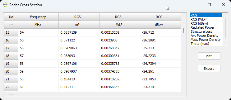
Far-Field Physics
These metrics are derived from the scattered field pattern in the far-field region. In this zone:
- The scattered field amplitude decays at a rate of $1/r$.
- The scattered power density decays at a rate of $1/r^2$.
Plotting Results
To visualize the frequency response of a specific parameter:
- Select the desired item from the list in the upper-right corner of the dialog box.
- Press the Plot button to display the data in AN-XY Chart.
To perform post-processing in external software or for detailed documentation, AN-SOF allows you to tabulate and export both spatial patterns and frequency spectra.
Available Export Commands
Navigate to the Results menu to access the following options:
- List Far-Field Pattern: Displays the spatial distribution of the radiation (gain, directivity, or field strength) at a specific frequency for a range of angles (Theta, Phi).
- List Far-Field Spectrum: Displays the far-field results across the entire simulated frequency range for a fixed observation direction (Theta, Phi).
The Results Table
Once you execute a command, a results window will appear (Fig. 1). This table includes:
- Angles: Theta and Phi coordinates.
- Electric Field Components: E-total, E-theta, E-phi, E-right, E-left (real and imaginary parts as well as magnitudes and phases).
- Axial Ratio: The axial ratio of the field polarization ellipse (dimensionless and in decibels).
Saving Data
To save this information for use in Excel, MATLAB, or Python:
- Click the Export button of the results window (Fig. 1).
- Choose a destination and save the file in CSV (Comma Separated Values) format.
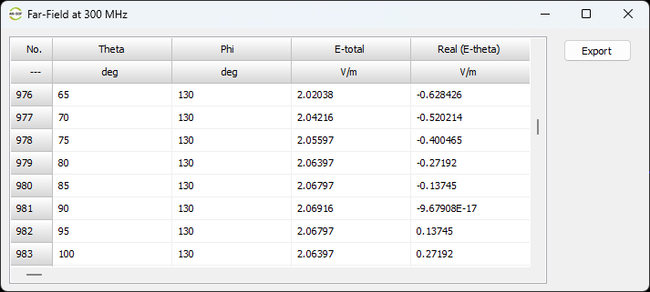
Near Field
In AN-SOF, near-field analysis allows you to evaluate the electric ($\mathbf{E}$) and magnetic ($\mathbf{H}$) fields in the immediate vicinity of an antenna or at any specified distance. This is essential for studying antenna-to-antenna coupling or electromagnetic compatibility (EMC).
Defining the Calculation Grid
Before plotting, you must define the observation points in the Near-Field panel of the Setup tab. You can specify the grid using:
- Cartesian Coordinates (X, Y, Z)
- Cylindrical Coordinates (R, Phi, Z)
- Spherical Coordinates (R, Theta, Phi)
Verification in the Far-Field
While these are “near-field” tools, they can be used to verify far-field behavior. As you move further from the antenna, you should observe:
- $\mathbf{E}$ and $\mathbf{H}$ becoming perpendicular to each other and the radial direction.
- Fields oscillating in phase.
- The intrinsic impedance of free space: $|\mathbf{E}| / |\mathbf{H}| \approx 120\pi\ \Omega \approx 377\ \Omega$.
Power Density and Compliance
If both $\mathbf{E}$ and $\mathbf{H}$ fields are calculated, AN-SOF provides the RMS Power Density ($S$), calculated as:
$S \,=\, |\mathbf{E} \times \mathbf{H}^*|$
This metric is critical for ensuring that your design complies with human exposure limits (e.g., ICNIRP or FCC standards).
3D Visualization
To visualize the fields as a 3D color-coded map, use the following paths in the main menu:
- Electric Field: Results > Plot Near E-Field Pattern > 3D Plot
- Magnetic Field: Results > Plot Near H-Field Pattern > 3D Plot
- Power Density: Results > Plot Power Density Pattern > 3D Plot
These commands launch AN-3D Pattern (Fig. 1). If your simulation includes multiple frequencies, you will be prompted to select a specific frequency before the plot is rendered.
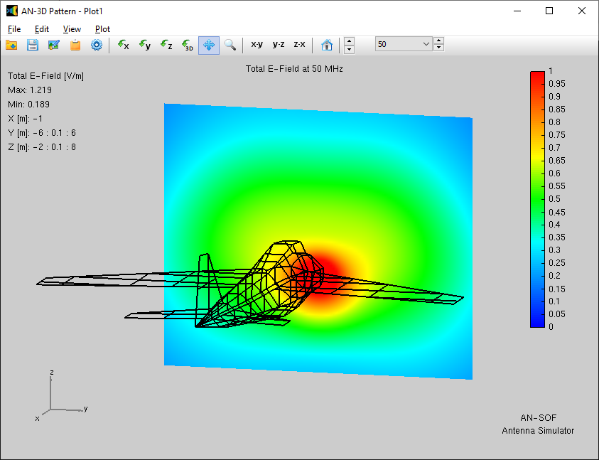
2D Visualization and Individual Components
For a more detailed look at field gradients along a specific axis or path, use the 2D Plot options under the same Results menus. This launches AN-XY Chart.
- Total RMS: The default view shows the total magnitude.
- Individual Components: You can isolate specific vectors (e.g., $E_x, E_y, E_z$) by navigating to the Plot menu within AN-XY Chart (Fig. 2).
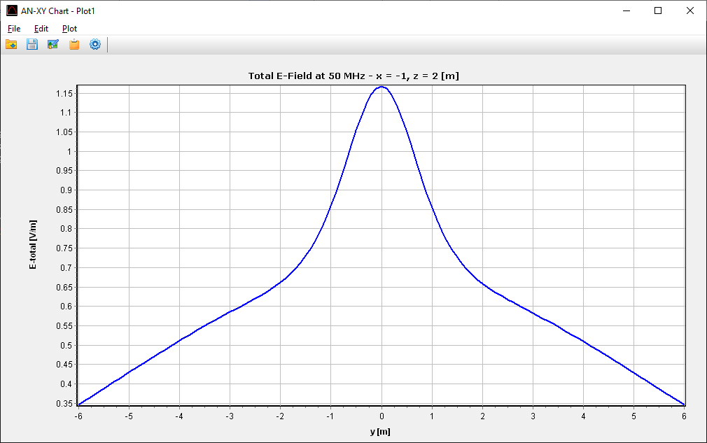
Tabulating and Exporting Data
To see the exact numerical values at every grid point, use:
- Results > List Near E-Field Pattern
- Results > List Near H-Field Pattern
- Results > List Power Density Pattern
These tables can be exported for further analysis in external mathematical tools.
Understanding Field Components by Coordinate System
The components of the electric and magnetic fields calculated by AN-SOF depend entirely on the coordinate system you select in the Near-Field panel of the Setup tab. Choosing the right system is crucial for matching the grid to the physical symmetry of your antenna.
1. Cartesian Coordinates $(x, y, z)$
When you select a rectangular grid, the fields are decomposed into their standard orthogonal components. This is ideal for planar structures or when evaluating fields along a straight line or over a flat surface.
- Electric Field Components: $E_x, E_y, E_z$
- Magnetic Field Components: $H_x, H_y, H_z$
2. Cylindrical Coordinates $(\rho, \phi, z)$
This system is best suited for structures with axial symmetry, such as vertical monopoles or circular arrays. The components are calculated relative to the radial distance from the $z$-axis and the rotation around it.
- Electric Field Components: $E_\rho$ (radial), $E_\phi$ (azimuthal), $E_z$ (axial)
- Magnetic Field Components: $H_\rho, H_\phi, H_z$
3. Spherical Coordinates $(r, \theta, \phi)$
Spherical coordinates are typically used to analyze how fields radiate outward into space. This setup is perfect for visualizing how near-fields begin to transition into far-field patterns.
- Electric Field Components: $E_r$ (radial), $E_\theta$ (zenith/elevation), $E_\phi$ (azimuth)
- Magnetic Field Components: $H_r, H_\theta, H_\phi$
Tip
In the AN-XY Chart application, you can isolate these individual components via the Plot menu to see which specific orientation contributes most to the total field magnitude at a given point.
While spatial plots show you how fields vary across a region at a single frequency, the Near Field Spectrum allows you to observe how the field intensity changes at a single, fixed point across a range of frequencies. This is essential for identifying resonant frequencies or ensuring field limits are not exceeded over a wide bandwidth.
Step 1: Selecting the Observation Point
Since a spectrum requires a stationary point, executing the plot command will first prompt the Select Near-Field Point dialog box (Fig. 1).
- To start, navigate to Results > Plot Near [E-Field/H-Field/Power Density] Spectrum.
- In the dialog box, select one of the points from the grid you previously defined in the Near-Field panel of the Setup tab.
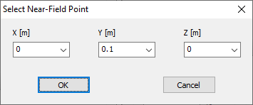
Step 2: Analyzing the Spectrum in AN-XY Chart
Once a point is selected, AN-XY Chart launches to display the magnitude of the field vs. frequency (Fig. 2).
To perform a deeper analysis of the vector components, you can use the Plot menu in the AN-XY Chart main menu to view:
- Components: Isolate $E_x, E_y, E_z$ (or the corresponding components for your chosen coordinate system).
- Data Types: Switch between Amplitude, Phase, Real, and Imaginary parts.
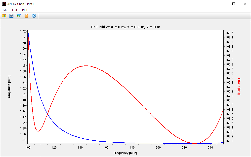
Practical Application
This feature is particularly useful when checking for Electromagnetic Interference (EMI). For instance, if you have sensitive electronics located at a specific distance from an antenna, you can plot the Power Density Spectrum at that exact coordinate to ensure it stays below a safe threshold across the entire operating frequency range.
For users who need to perform external numerical analysis or generate reports, AN-SOF provides a straightforward way to move near-field data into tools like Excel, MATLAB, or Python.
Available Export Commands
Access these options via the Results menu. Depending on whether you need spatial data (at a specific frequency) or frequency data (at a specific point), choose from the following:
- List Near E-Field/H-Field/Power Density Pattern: Displays a table of the electric field ($\mathbf{E}$), magnetic field ($\mathbf{H}$), or power density ($S = |\mathbf{E} \times \mathbf{H}^*|$) across your entire grid for a single frequency.
- List Near E-Field/H-Field/Power Density Spectrum: Displays the field behavior across all simulated frequencies for a single, fixed coordinate point.
The Results Table
Executing these commands opens a data window containing the raw numerical results. The table format adapts to your chosen coordinate system:
| Column Type | Description |
| Coordinates | The position $(x, y, z)$, $(\rho, \phi, z)$, or $(r, \theta, \phi)$. |
| Total Field | The total RMS magnitude of the field at that location/frequency. |
| Field Components | Magnitude and Phase for each vector component (e.g., $E_x, E_y, E_z$). |
Saving to CSV
To export this data:
- Click the Export button on the right side of the table.
- Specify your file name and save it as a .csv file.
This format is universally compatible and allows you to recreate high-resolution heat maps or perform safety compliance calculations in third-party software.
Transmission Lines
Adding a transmission line to a model has an impact on the entire calculation, affecting current distribution, input impedance, and near and far fields. AN-SOF allows for the addition of lossy or lossless transmission lines and has a list of preloaded lines with parameters adjusted to the attenuation curves published in the data sheets of real cables. This list of cables includes both two-wire and coaxial transmission lines.
After drawing and segmenting the wire structure that will represent an antenna or an object that will scatter electromagnetic waves, the recommended first step is to create a list of the transmission lines that will be connected to the structure. This is described below.
The ends of a transmission line in AN-SOF are called Port 1 and Port 2 since a line can be considered as a two-port network. Each end or port of a transmission line can be connected to a segment of the wire structure, as Fig. 1 shows. A transmission line is defined by its characteristic impedance, Z0, velocity factor, VF, a loss model or attenuation curve, and shunt admittances, Y1 and Y2, connected across each port. Each transmission line must be connected between two different wire segments (the i-th and j-th segments in Fig. 1 should not be the same segment). In the calculation engine model, a gap is opened in the center of each segment to allow a transmission line to be connected there.
Transmission lines are modeled in an implicit way, meaning that the lines don’t scatter electromagnetic waves in space, but rather interact with the wire structure by establishing boundary conditions on the voltages and currents at the connected segments. Implicit modeling is adequate when the disturbance in the electromagnetic field caused by the physical presence of the transmission line can be neglected, e.g., for twisted-pair lines in most cases. On the other hand, explicit modeling involves drawing the two parallel wires of a two-wire line in the workspace and dividing them into segments, like the rest of the structure. For coaxial lines, a “hybrid” modeling approach can be used, which is explained in Modeling Coaxial Cables.
To add transmission lines, go to the AN-SOF main menu > Draw > Transmission Lines (Ctrl + L). A table will be displayed where a transmission line can be entered on each row. Follow the procedure below to enter the lines:
- Select a row by clicking on the row number of your choice in the first column labeled ‘No.’, Fig. 2.
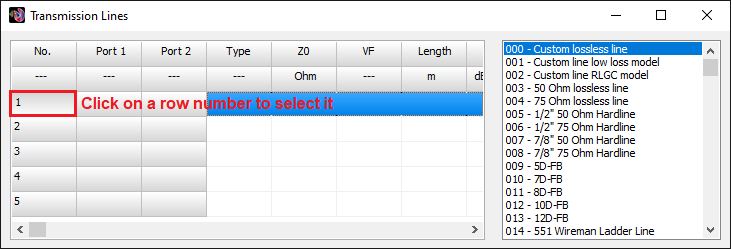
- On the right-hand panel, choose a type of transmission line and double-click on your chosen type. The selected row will be automatically completed, Fig. 3.
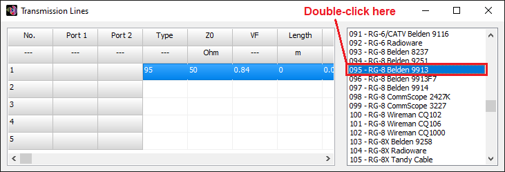
- From type 3 onwards, the parameters correspond to real cable datasheets. If you wish to enter your own parameters, choose types 0, 1, or 2. To edit the value in a cell, double-click on the cell.
Note that in this procedure, the ports of the transmission lines have not been connected to the wire segments yet. This is explained in Connecting Transmission Lines.
The parameters that define a transmission line are:
1) Type: On the right-hand panel of the Transmission Lines window, there is a list of lines with the cable part number and the manufacturer in some cases. The first three types are used to input user-customized lines. The line type simply refers to its position in this list.
2) Z0: Nominal characteristic impedance, in Ohms. If a negative value is entered, the transmission line will be “crossed” with a 180° phase reversal with respect to the reference directions of the segments (the characteristic impedance of the line will of course be |Z0|).
3) VF: Velocity factor (dimensionless). The allowed range is 0 < VF <= 1.
4) Length: Length of the line, in the unit selected in the Preferences window (see Section “3.3 Preferences”). If a length of zero is entered, the length of the transmission line will be equal to the linear distance between the two wire segments connected at the ends of the line.
5) The K0, K1, K2, and K3 columns define the line losses for the so-called RLGC model. These four columns will change to Att. 1, Freq. 1, Att. 2, Freq. 2 when the chosen line model is that of low losses. These cells allow entering the attenuation curve of a real transmission line from its datasheet.
6) Real(Y1) and Imag(Y1) are the real and imaginary parts of the shunt admittance through Port 1 of the transmission line, in Siemens [S].
7) Real(Y2) and Imag(Y2) are the real and imaginary parts of the shunt admittance through Port 2 of the transmission line, in Siemens [S].
A transmission line without shunt admittances (Y1 = Y2 = 0) will always be symmetrical in the sense that if it is connected in reverse, i.e., by swapping ports 1 and 2, the same results will be obtained in a simulation. Ports 1 and 2 are identified so that the locations of the shunt admittances can be distinguished when they are not zero.
If you enlarge or maximize the Transmission Lines window, you will be able to see the columns corresponding to the loss model parameters and shunt admittances, Figs. 4 and 5. Initially, this window only displays cells up to the ‘Length’ column so that the user does not have to worry about the loss parameter values since these are automatically loaded when selecting a line type from the list. Adding an attenuation curve when modeling a cable that is not on the list is explained in Adding a Custom Lossy Line.
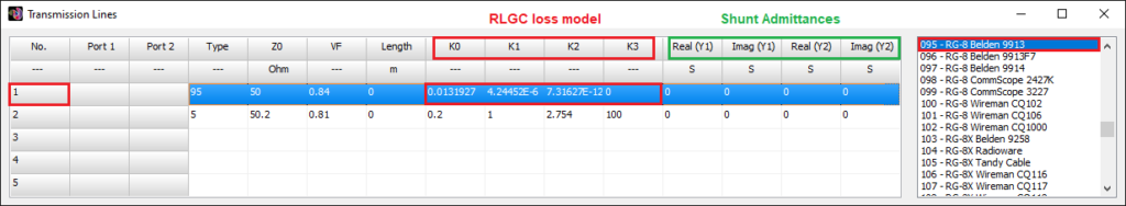
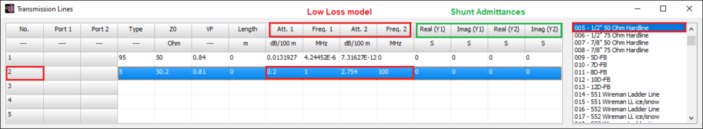
If you want to add “custom” transmission lines with your own parameters, you have types 0, 1, and 2 available, Fig. 1, which are explained below.
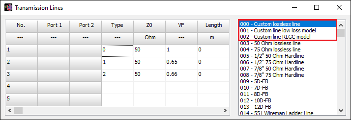
Type 0: Custom Lossless Line
This is an ideal transmission line with zero losses, so only the nominal Z0 and velocity factor must be specified.
Type 1: Custom line – low loss model
This is a transmission line where the nominal Z0, velocity factor, and matched loss curve can be specified. To define the matched loss curve, two attenuation values must be entered at two different frequencies, with the second frequency being greater than the first. AN-SOF will then adjust a low-loss model to obtain an attenuation vs. frequency curve for subsequent calculations. This is the simplest way to enter parameters from the datasheet of a manufactured real transmission line. Refer to Adding a Custom Lossy Line where it explains how to add the parameters from an attenuation curve published in a datasheet of a real cable.
Type 2: Custom line – RLGC model
This is a transmission line model that considers losses by adjusting a matched loss curve to the table of attenuation vs. frequency in the cable datasheet. The K0, K1, and K2 constants must be entered in this case. The definition of K0, K1, and K2 assumes that the frequency is in Hz and the lengths are in meters (SI metric units). This option allows for the entry of K0, K1, and K2 obtained from third-party transmission line calculators (K3 is an additional constant that is zero for all available cables).
Any transmission lines added through the Transmission Lines command (Ctrl + L) under the Draw menu will remain in the table until the user decides to remove or modify them. During calculations, only transmission lines with both ports connected to respective wire segments will be considered for simulation. Any lines with a single port connected or both ports disconnected will be omitted in the calculations.
To connect a transmission line between two wire segments, follow these steps:
- Right-click on the first wire to select it and choose the Source / Load / TL (Ctrl + Ins) command from the pop-up menu. This will open a horizontal toolbar with a slider control, Fig. 1.
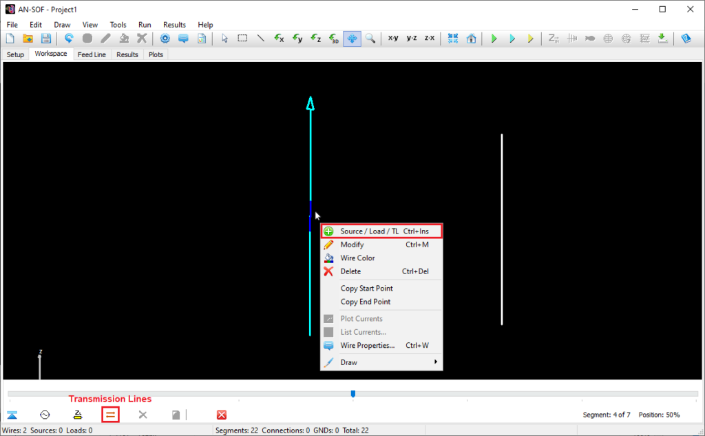
- Use the slider to select the specific segment of the first wire to which you want to connect a port of the transmission line.
- Once you’ve chosen the segment, click on the Transmission Lines button on the horizontal toolbar to open the Transmission Lines table, Fig. 2.
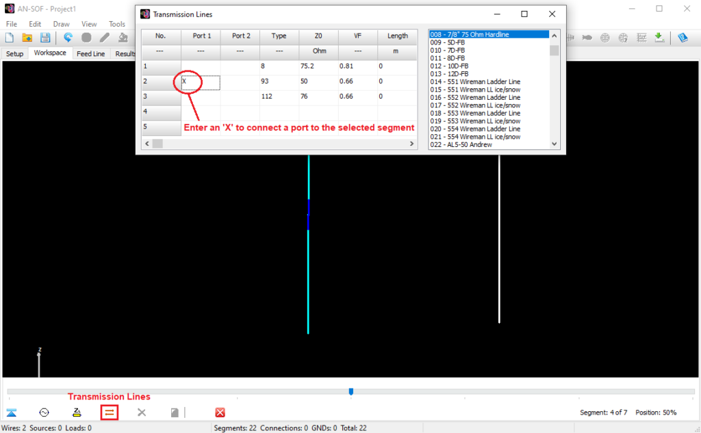
- Enter an “x” or “X” (without quotes) in the corresponding cell for the port you want to connect to the selected segment (the cells located below the “Port 1” and “Port 2” columns), Fig. 2. You can enter an “X” for all the ports that need to be connected to the same segment as multiple transmission lines can be connected to it. Finally, close the Transmission Lines window.
- Select the second wire and repeat steps 1-4 to connect the second port of the transmission line to another segment, Fig. 3. The transmission lines with both ports connected will be graphically displayed as shown in Fig. 4.
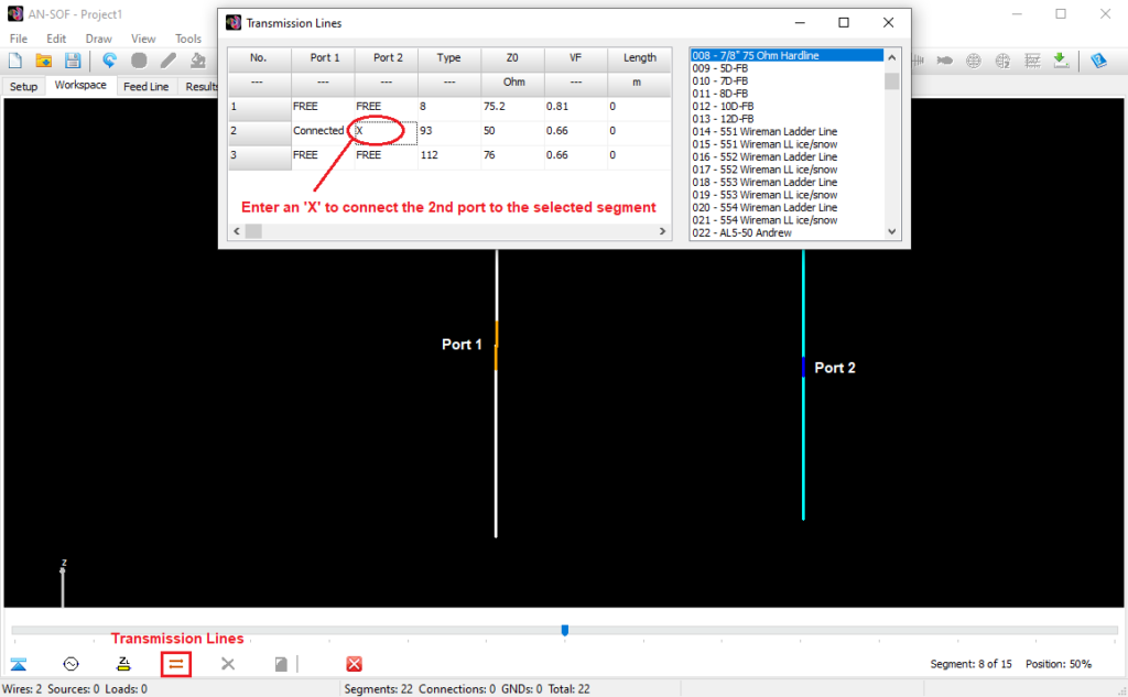
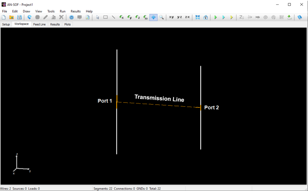
While performing this procedure, you have the option to add more transmission lines directly in the “Transmission Lines” dialog window. This saves you from having to follow the steps outlined in Adding Transmission Lines. The advantage of adding transmission lines here is that you can edit the connections of the lines in the “Port 1” and “Port 2” columns. However, with the Draw > Transmission Lines (Ctrl + L) command, you can quickly edit the lines (Z0, VF, length, etc.) if you don’t need to change the port connections.
A port that is already connected to a segment will show the status as “Connected,” while if it is not connected to any segment, it will display the status as “FREE”. When we are on a selected segment, a connected port will show the status as “Here,” which refers to the port being connected specifically to that selected segment.
To disconnect a port from a segment, enter the word “FREE” (without quotes, in uppercase) in the corresponding cell instead of an “X”. This allows you to use the “X” and “FREE” commands to easily connect and disconnect ports on a selected segment.
The transmission lines that have both ports connected to segments are displayed as straight dashed lines in orange color in the workspace, Fig. 4. An arrow will indicate the direction of the line, which goes from port 1 to 2. Since the length of a line is another parameter that is entered, such as its characteristic impedance and velocity factor, the length of the line in the workspace may not represent the configured or “real” length of the line.
If you select a row by clicking on the row number in the Transmission Lines table, the corresponding line will be highlighted in red in the workspace (if it has both ports connected to segments), Fig. 5. This way, you can visually identify which line you are editing.
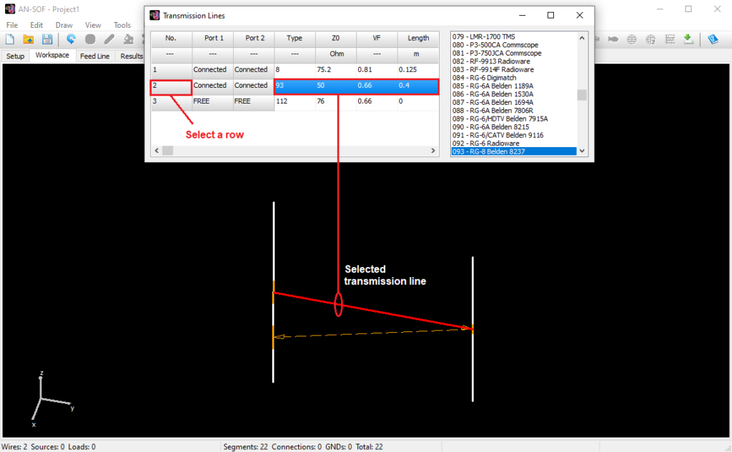
IMPORTANT Information
- A transmission line with only one port connected to a wire segment will not be considered in the calculations. Instead, it exists as a row within the table, which can be used as a library of lines to select from and connect to the wire structure. Therefore, when a port is FREE, it does not mean that the corresponding end of the transmission line is open circuited, but rather that this line will simply be omitted in the simulation. It is sufficient for only one port to be FREE for the line to be omitted. If you need to connect a line with an open or short-circuited end, please refer to Open and Short-Circuited Lines for detailed instructions.
- A voltage or current source can be connected to any segment where one or more transmission line ports are connected. In this case, the sources will always be “ideal”, i.e., with zero/infinite internal impedance (zero for voltage sources and infinite for current sources), unlike in an ordinary segment without a port connected, where sources may have non-zero/finite internal impedance (in AN-SOF, current sources should always have a finite internal impedance because this impedance is connected in parallel with the current source).
- In each segment, only transmission line ports or a load impedance are allowed, but not both. If a port is connected to a segment where a load impedance already exists, this impedance will be eliminated, and vice versa. If you need to connect a load impedance in series with the port of a transmission line, connect the impedance in an adjacent segment to the port.
- When there are transmission lines in the model, the NGF (Numerical Green’s Function) option will be automatically enabled in the Settings panel of the Setup tabsheet. This way, calculations will be performed faster in the next simulation if only the parameters of the transmission lines are modified while the wire structure remains unchanged.
- It is recommended to connect transmission lines after drawing and segmenting the wire structure. If the number of segments changes, the lines may become disconnected and need to be manually reconnected using the procedure described in this section.
- To ensure a smooth calculation process, AN-SOF will verify the correct connections between the transmission lines and the wire segments. If AN-SOF detects any errors, it will promptly remove the faulty connection by setting the corresponding port to FREE state.
Due to the model used in the calculation engine, the transmission lines that are considered to exist in the simulation are those that have both ports connected to wire segments. Therefore, if you want to have an open-circuited line connected to a certain segment, the opposite port must also be connected to another wire segment. Create a short wire with only one segment that is no longer than 1% of the wavelength (its radius can be one-tenth of its length) and connect it to the open circuit transmission line port. This short wire should be disconnected from the rest of the structure, and the shunt admittance of the port it’s connected to should be zero, Fig. 1.
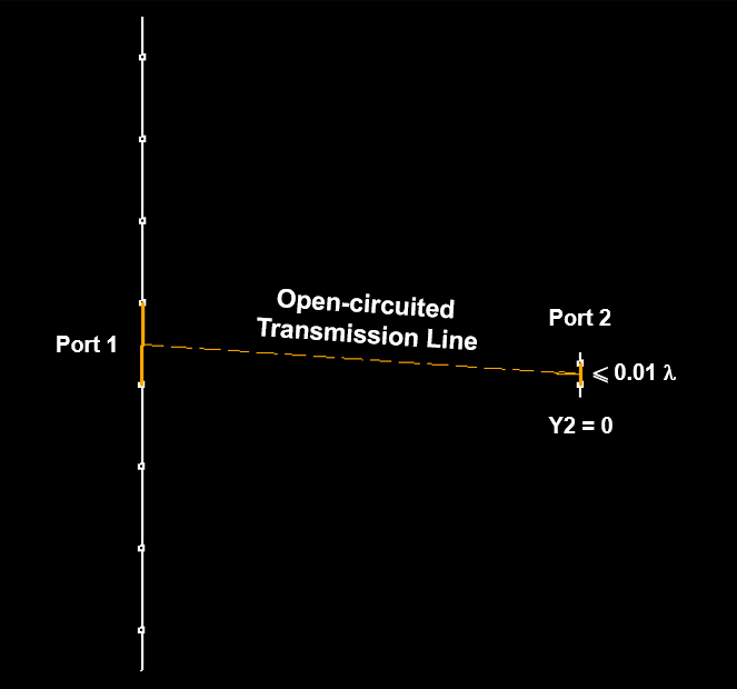
On the other hand, if you need a transmission line with a short-circuited port, connect that port to any other segment and set a shunt admittance at that end that is very large, for example, 1E6 [S]. At this end, you could connect a short wire segment created for this purpose, as is done for an open-circuited line, Fig. 2.
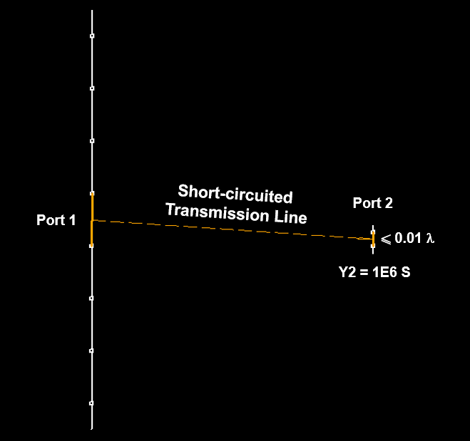
When creating short wires to connect open or short circuit transmission line ports, it is advisable to move these wires away from the rest of the structure to minimize interaction with it. Enter the length of the transmission line as indicated in Adding Transmission Lines. Remember that the length of the line is not necessarily related to the actual distance between the segments where it is connected.
The Transmission Lines table has a pop-up menu with keyboard shortcuts, Fig. 1. To access this menu for editing cells and rows, right-click on the table. The available commands are:
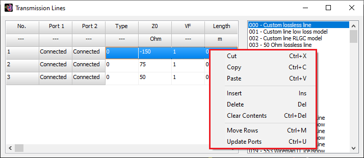
- Standard Cut (Ctrl + X), Copy (Ctrl + C), and Paste (Ctrl + V) options are available for cells. A single cell can be selected by left clicking on it or by using the TAB and arrow keys on the keyboard.
- To select a row, click on the row number in the left column (the “No.” column). Use the mouse or the up and down arrow keys on the keyboard to select a single row. Double-click on a single cell to exit row selection mode.
- Cut (Ctrl + X), Copy (Ctrl + C), and Paste (Ctrl + V) options also apply to a selected row. In addition, Insert (Ins key) and Delete (Del key) options can be used to add or remove rows.
- The Clear Contents (Ctrl + Del) command clears the content of a selected cell or row.
- The Move Rows (Ctrl + M) command allows you to enter a mode where rows can be moved up or down to order them as desired. To exit this mode, click Move Rows (Ctrl + M) again.
- The Update Ports (Ctrl + U) command checks and updates the status of the transmission line ports. Use this command to verify that the lines have their ports connected to wire segments when you have made any modifications to the segmentation or geometry of the wires where there are transmission line ports.
Coaxial transmission lines can be modeled implicitly, as explained in previous articles. To define a coaxial cable, one needs to know its characteristic impedance (Z0), velocity factor (VF), length, parameters that model losses (K0, K1, K2, etc.), and the shunt admittances at each end (Y1 and Y2). Additionally, each end or port of the line must be connected to the center of a wire segment. In this implicit model, the electromagnetic interaction between the coaxial cable shield and the wire structure is neglected, and the line ends impose boundary conditions on the voltage and current in the connected segments. However, in certain scenarios, a current can be induced that flows through the outside of the coaxial cable shield, known as common-mode current, and this current cannot be neglected. To address this, a hybrid model is used, which is explained in detail below.
In the hybrid model, the internal behavior of a coaxial cable is implicitly modeled using its parameters such as Z0, VF, length, etc. On the other hand, the outer shield is modeled by adding a wire that must be divided into segments like the rest of the structure, Fig. 1. This additional wire considers the current induced outside the coaxial cable shield.
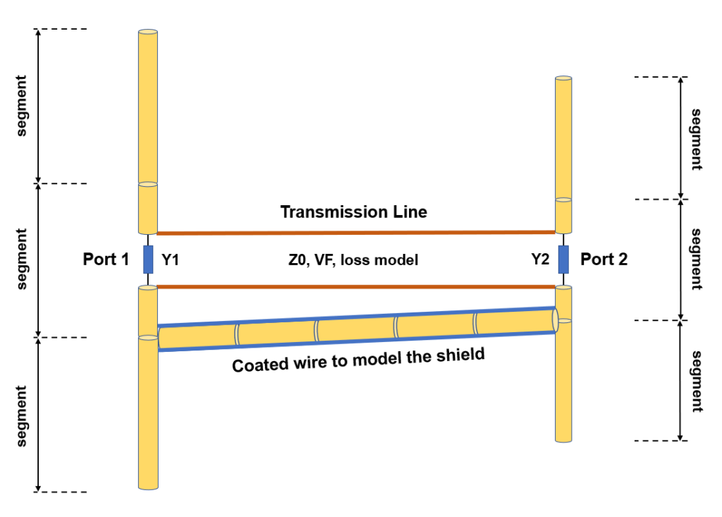
The wire representing the shield should be connected between two ends of the segments where the cable is connected, Fig. 2. Unlike transmission lines that connect in the center of the segments, wires are connected at their ends. Hence, the additional wire representing the shield will be a segment offset from the actual position of the cable. This is not a significant concern since the segments should be small compared to the wavelength.
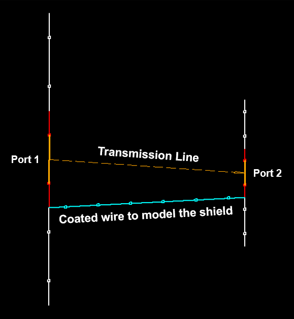
Please be reminded that to connect one wire to another and connect the ends of the coaxial cable shield, you will need to manually divide the wires involved, as explained in Connecting Wires.
To simulate the dielectric coating of actual coaxial cables, an outer insulation can be added to the wire representing the shield, and its thickness can be input as well.
AN-SOF provides parameters for modeling the losses of more than 160 types of transmission lines. These parameters have been obtained by adjusting the loss model to the attenuation curves published by manufacturers. In case a particular type of cable is not listed or if the manufacturer has updated the parameters, a custom transmission line can be created using the following procedure:
- Open the Transmission Lines window by going to the main menu > Draw > Transmission Lines (Ctrl + L) or follow the procedure in Connecting Transmission Lines to open this window by selecting a wire.
- Select a row from the table by clicking on the row number (under the first column labeled No.).
- In the panel on the right, double-click the Custom line low loss model option.
- All manufacturers publish the nominal characteristic impedance, Z0, and the velocity factor, VF. Enter these values as well as the length of the line. If you enter “0” in the length cell, the linear distance between the ends of the cable will be calculated.
- Manufacturers also publish an attenuation table as a function of frequency. Here is an example for the Belden 8237 cable, type RG-8/U:
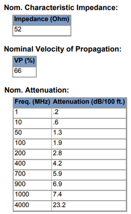
- In the cells corresponding to Att. 1, Freq. 1, Att. 2, and Freq. 2, enter the values from the attenuation table so that the simulation frequency range is included between Freq. 1 and Freq. 2. For example, if you are running a calculation between 150 and 170 MHz, enter Att. 1 = 1.9 dB/100 ft, Freq. 1 = 100 MHz, Att. 2 = 2.8 dB/100 ft, Freq. 2 = 200 MHz, as indicated in the table for the Belden 8237 cable, Fig. 1.
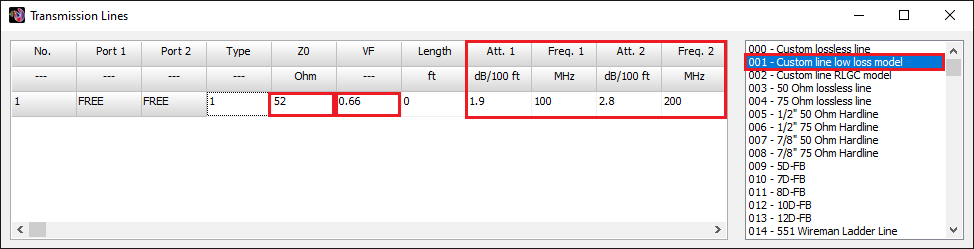
Be careful with the units of attenuation and frequency, as they will be displayed in the units chosen in the Preferences window. Go to main menu > Tools > Preferences > Units tab to change the units for frequency and length.
Step By Step
The Models tab in the AN-SOF interface provides a categorized library of pre-built antenna projects. These serve as excellent starting points for learning how to use the software effectively (Fig. 1).
Interactive Learning
When you click on a model button:
- Instant Visualization: The project opens immediately, displaying the 3D radiation pattern and geometry.
- Documentation: A detailed PDF document opens automatically, explaining the underlying physics and the specific configuration of that model.
Trial Version Compatibility
The trial version of AN-SOF has a 50-segment limit (totaling wire segments, junctions, and ground connections). Here is how you can use the examples:
- View Mode: All pre-computed example models, even those exceeding 50 segments, can be opened in the Trial version. You can fully inspect the 3D plots, tables, and graphs of these existing results.
- Run Mode: To run a new calculation or modify a design, the model must stay within the 50-segment limit.
- Downloadable Models: You can download these five specific models designed for the trial version:
- 2-Element Quad
- 2-Element Delta Loop
- HF Skeleton Slot
- Inverted V
- 5-Element Yagi-Uda
Expanding Your Knowledge
- Knowledge Base: Visit the website’s Knowledge Base for comprehensive articles with dedicated category filters.
- Resources & Blog: Check these pages frequently for the latest downloadable examples and engineering insights: Resources and Antennas Blog.
- Newsletter: Subscribe to “Antennas and Beyond!” to receive updates, project ideas, and new models directly in your inbox.
Discover 5 antenna models with less than 50 segments in AN-SOF Trial Version. These examples showcase the capabilities of our software for antenna modeling and design, allowing you to evaluate its features for your projects.
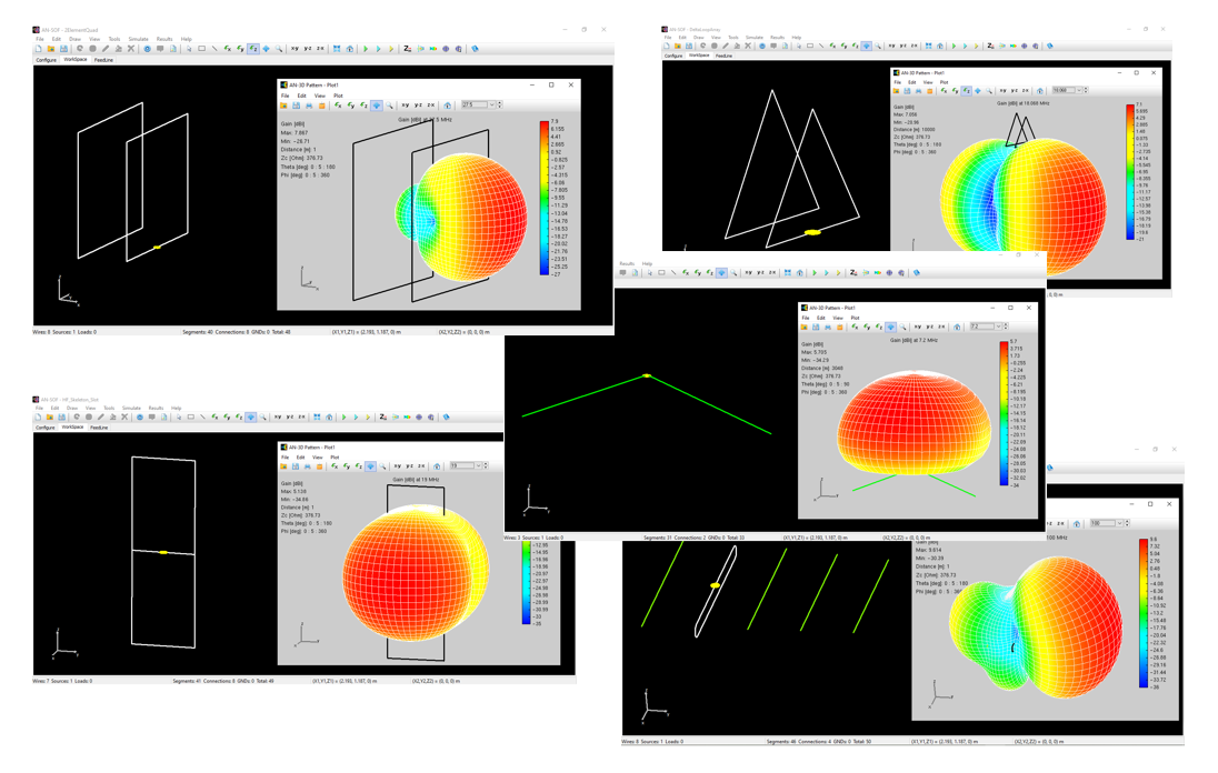
The trial version of AN-SOF is fully featured and has no expiration date. It allows users to open any pre-calculated example file to inspect data tables and visualize 3D radiation patterns and graphs. The sole limitation is the calculation capacity, which is capped at 50 “unknowns.” In this context, an unknown represents an electric current value to be determined by the AN-SOF engine at each segment, junction, or ground connection. Consequently, the sum of segments, wire-to-wire connections, and ground connections must not exceed 50 to run a new simulation in the Trial version.
The purpose of the trial version is to allow users to evaluate the full features and capabilities of AN-SOF for antenna modeling and design. You can access a variety of pre-calculated models directly through the Models tab in the software. Furthermore, our Knowledge Base features an extensive collection of model examples accompanied by descriptive articles. These resources are categorized by antenna type, ranging from fundamental wire structures to antennas situated in complex environments.
For more complex antenna designs, the 50-unknown limit may be reached quickly. While users can view pre-calculated examples that exceed this threshold, any modifications requiring a re-run of the simulation will be restricted if the total number of segments and connections exceeds 50. Nevertheless, the trial version remains a highly effective tool for simulating fundamental antenna projects or structures with small electrical dimensions relative to the wavelength.
Download the following 5 example models with less than 50 segments to make modifications to the antenna structures:
- 2 Element Quad
- 2 Element Delta Loop
- HF Skeleton Slot
- Inverted V
- 5 Element Yagi-Uda
To ensure reliable results, a minimum of 10 segments per wavelength should be used. For antennas that are highly sensitive to element lengths, such as Yagi-Uda arrays, a higher density of approximately 50 segments per wavelength is recommended to achieve results that closely align with physical VSWR measurements.
Explore further case studies and technical articles in the Validation section of our Knowledge Base. Additionally, the AN-SOF Trial Version features integrated tuner and feeder calculators, enabling users to synthesize impedance matching networks, incorporate transformers, and determine optimal feed line parameters for any given load impedance.
Ultimately, AN-SOF Trial offers a robust platform for antenna simulation, providing all the necessary tools to evaluate its performance and capabilities. With access to pre-calculated examples and advanced design utilities, users can navigate the complexities of antenna design with ease.
See Also:

Learn how to simulate a center-fed cylindrical antenna using AN-SOF software. This step-by-step guide covers setup, geometry creation, simulation, and result analysis. Understand dipole characteristics through practical examples.
Introduction: Center-Fed Cylindrical Antenna Simulation
The center-fed cylindrical antenna serves as a fundamental example for simulation. Essentially a straight wire with a central excitation, it transitions into a half-wave dipole when its length aligns with half the wavelength of the operating frequency. The following steps outline the simulation process using AN-SOF.
Step 1: Configuring the Simulation Environment
To initiate, navigate to Tools > Preferences within the main menu to establish appropriate units for frequency (MHz) and length (m). Subsequently, access the Setup tab. Within the Frequency panel, select Sweep and configure the Frequency Sweep parameters as depicted in Fig. 1. The calculations will be performed at the frequencies: 50, 55, …, 295, 300 MHz. Ensure that None (free space) is chosen in the Environment panel‘s Ground Plane box and Discrete Sources is selected under the Excitation panel.
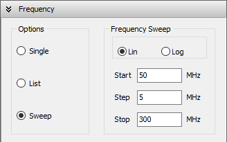
Step 2: Creating the Antenna Geometry
To initiate the antenna geometry creation, right-click within the workspace and select Line from the ensuing pop-up menu. The ‘Line’ dialog box will appear. Populate the Line and Attributes pages as outlined in Figs. 2 and 3 to generate a straight wire comprising 17 segments and a 1 mm radius within the workspace. The wire will be drawn starting from point (0,0,-0.75) [m] and ending at point (0,0,0.75) [m], aligning with the z-axis and spanning a length of 1.5 m, equivalent to a half-wavelength at 100 MHz. Press F7 to visualize the primary axes.
Subsequently, right-click on the wire and choose Source/Load/TL from the context menu. Following the procedure detailed in “Adding Sources,” introduce a voltage source at the wire’s center (segment 9). Set the source voltage to 1 (0°) V. The resulting center-fed cylindrical antenna in the AN-SOF’s workspace is represented in Fig. 4.
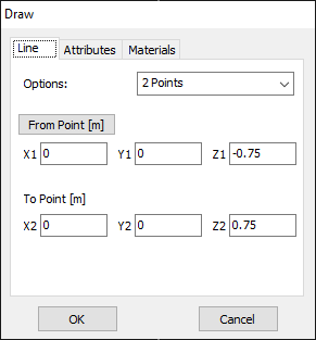

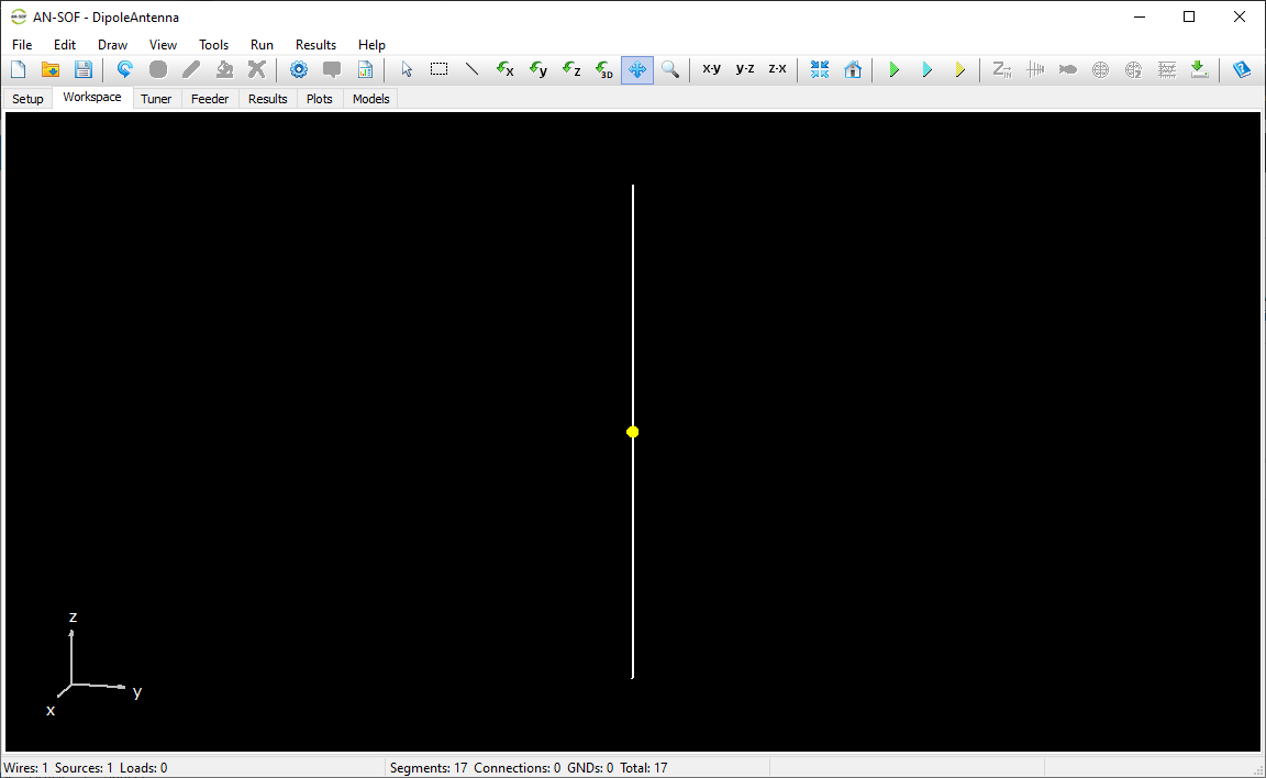
Step 3: Simulation Execution and Result Analysis
To initiate the simulation process, click the Run Currents and Far-Field (F11) button on the toolbar. Upon completion, right-click on the wire and select Plot Currents from the context menu, specifying the desired frequency. The resulting current distribution along the wire is graphically represented in Fig. 5. To access additional parameters of interest, refer to the procedures outlined in “Displaying Results.”
As an illustrative example, Figures 5, 6, and 7 depict the current distribution at 100 MHz (amplitude in Fig. 5(a) and phase in Fig. 5(b)), input impedance versus frequency (real part in Fig. 6(a) and imaginary part in Fig. 6(b)), and gain pattern in dBi (Fig. 7) at 100 MHz.
Given that the antenna length (1.5 m) equals half a wavelength at 100 MHz, the current distribution in amplitude approximates a half-cycle sine function, aligning with the expected behavior of a half-wave dipole. A slight decrease in the amplitude and a sharp increase in the phase can be seen at the antenna center, due to the presence of the voltage source just there. The presence of the voltage source at the center disrupts the continuity of the current’s slope (derivative) at that point, while the current itself remains continuous.
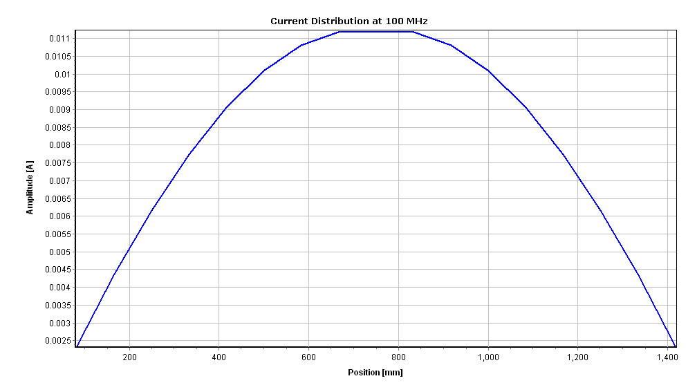
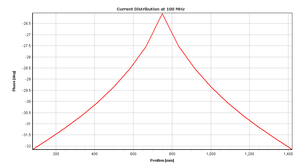
If we look closely at Figure 6(b), which shows the input reactance (imaginary part of the input impedance), we can see that the curve crosses zero just before 100 MHz, with a positive slope (series resonance), then crosses zero again just above 180 MHz, with a negative slope (parallel resonance), and then crosses zero again just below 300 MHz with a positive slope (series resonance). These three points where the reactance vanishes correspond to when the physical length of the dipole approaches: λ/2, λ, and 3λ/2. The resonances do not occur exactly at integer values of half wavelength because the thickness of the dipole is not infinitesimal. In Figure 6(a) we can see that the input resistance is maximum at the frequency that corresponds to the parallel resonance. All these are the expected and classical behaviors of a dipole of finite thickness.
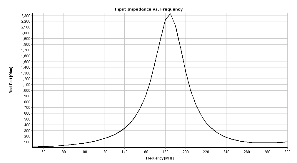
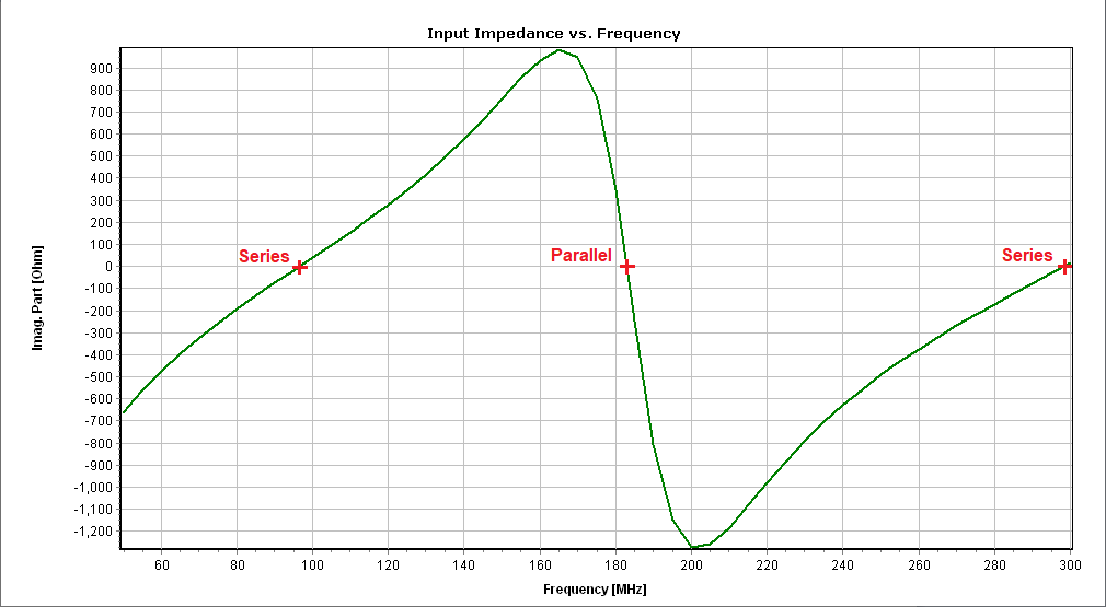
Regarding the gain pattern in Fig. 7, it is donut-shaped as expected for a half-wave dipole, with a maximum of 2.17 dBi. We should remember that the theoretical peak gain of an infinitesimally thin half-wave dipole in free space with a perfect sinusoidal current distribution is 2.15 dBi (corresponding to a numerical gain of 1.64). The obtained gain in AN-SOF is 0.02 dBi higher than the theoretical value due to the finite radius of the cross-section of the dipole.
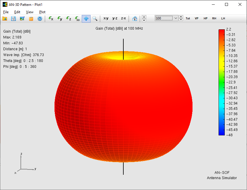
Conclusion
This tutorial provided a step-by-step guide to simulating a center-fed cylindrical antenna using AN-SOF Antenna Simulator. By following the outlined procedures, users can efficiently model this fundamental antenna type and analyze its key characteristics.
The simulated results align with the expected behavior of a half-wave dipole, demonstrating the software’s accuracy in predicting current distribution, input impedance, gain, and radiation patterns. The influence of the antenna’s finite thickness on the resonance frequencies and gain was also highlighted.
This example serves as a foundation for more complex antenna designs. By understanding the simulation process for this simple geometry, users can apply similar principles to model and analyze a wide range of antenna structures.
See Also:
This step-by-step guide empowers you to simulate circular loop antennas in AN-SOF. We’ll configure the software, define loop geometry, and explore how its size relative to wavelength affects radiation patterns and input resistance. Gain valuable insights into this fundamental antenna type!
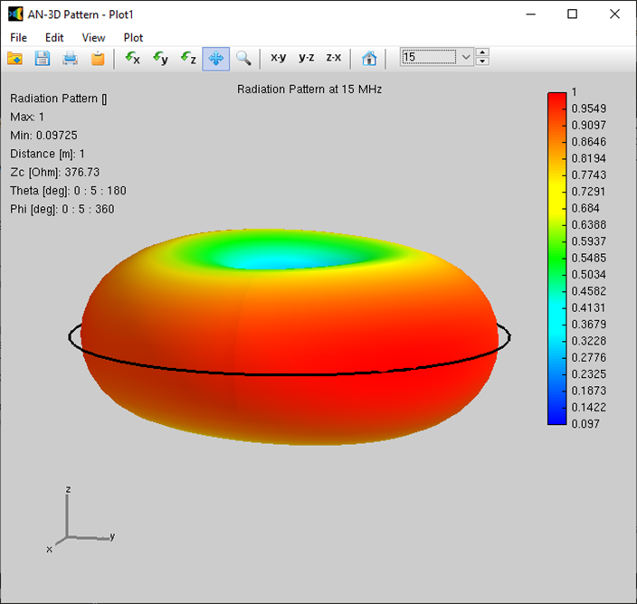
This article provides a step-by-step guide to modeling a circular loop antenna using AN-SOF software. Circular loops are a common antenna type, and their analysis requires curved segments within the simulation environment. The guide will detail the configuration process, including defining the loop geometry, setting up the frequency sweep, incorporating a voltage source, and analyzing the key parameters like radiation pattern and input resistance. This guide is valuable for RF engineers, ham radio enthusiasts, students, and antenna design professionals seeking to utilize AN-SOF for circular loop antenna simulations.
1. Specifying the Simulation Setup
This section outlines the initial setup steps required to model a circular loop antenna in AN-SOF. We’ll configure a frequency sweep to analyze the antenna’s behavior across a specified range.
Frequency Sweep:
- Navigate to the Setup tab and select Sweep within the Frequency panel.
- Choose Lin for a linear frequency sweep. This allows for evenly spaced data points across the desired range.
- Define the sweep parameters:
- Start frequency: 3 MHz
- Step: 1 MHz (adjust as needed based on desired resolution)
- Stop frequency: 30 MHz
These settings establish a linear sweep from 3 MHz to 30 MHz with 1 MHz increments between each data point (as shown in Fig. 1).
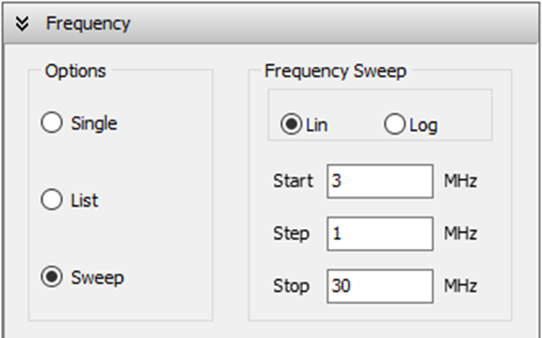
Additional Settings:
- Environment: Ensure that None is selected in the Ground Plane box within the Environment panel. This removes any ground plane influence from the simulation, which might not be relevant for a free-space loop antenna.
- Excitation: In the Excitation panel, verify that Discrete Sources is selected. This indicates that we’ll define a lumped source (voltage or current) to excite the antenna later in the modeling process.
By following these steps, we’ve established the foundation for our loop antenna simulation by configuring the frequency sweep and essential simulation settings in AN-SOF. The next section will delve into defining the geometry of the circular loop itself.
2. Defining the Circular Loop Geometry
This section focuses on creating the circular loop geometry within the AN-SOF workspace:
- Access the Draw Menu: Navigate to the Workspace tab. Right-click on an empty area within the workspace and select Circle from the pop-up menu.
- Specify Loop Parameters: The Draw dialog box for the circle will appear (Fig. 2). Define the following parameters for your loop antenna using the provided tabs:
- Center: (Cx, Cy, Cz) = (0, 0, 0) (Circle tab)
- Radius: 0.5 meters (Circle tab)
- Segments: 8 (Attributes tab)
- Cross-section type: Circular (Attributes tab)
- Cross-section radius: 5 millimeters (Attributes tab)
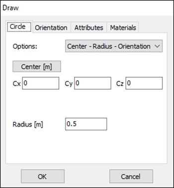
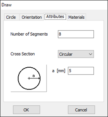
Segment Selection: The number of segments used to discretize the loop circumference is crucial for accurate simulation results. While 8 segments are a reasonable starting point, a convergence study might be necessary to ensure sufficient accuracy, especially for electrically large loops. As a rule of thumb, aim for 10-20 segments per wavelength at the highest frequency of interest.
Electrical Size Considerations: It’s important to consider the loop’s electrical size relative to the wavelength. At 30 MHz (the highest frequency in your sweep), the wavelength (λ) is indeed 10 meters, and the loop’s circumference (0.314λ) is close to one-third of a wavelength. This suggests the loop might not be electrically small at the high end of the frequency range. This characteristic will affect the antenna input impedance and radiation pattern.
Assigning the Excitation Source:
- Right-click on the circular loop within the AN-SOF workspace.
- From the pop-up menu, select Source/Load.
- Choose to add a voltage source and position it at the first segment of the loop.
For detailed instructions on source placement and parameter definition, refer to the AN-SOF documentation’s ‘Adding Sources‘ section.
3. Running the Simulation and Analyzing Results
This section guides you through initiating the simulation process and analyzing the obtained results in AN-SOF:
- Run Simulation: Locate the Run Currents and Far-Field (F11) button on the toolbar and click it. This initiates the simulation, calculating the current distribution on the loop and its far-field radiation pattern across the defined frequency sweep.
- Visualizing the Radiation Pattern: Once the simulation is complete, click the Far-Field 3D Plot button on the toolbar. This will display the radiation pattern of the loop antenna in a 3D format (AN-3D Pattern application similar to Fig. 3).
- Frequency-Dependent Analysis: The AN-3D Pattern toolbar offers functionalities to explore the radiation pattern’s behavior at different frequencies within the sweep range.
- Frequency selection dropdown menu: This menu allows you to directly choose a specific frequency point to view its corresponding radiation pattern.
- Frequency navigation buttons: Utilize the up and down arrow buttons on the toolbar to navigate through the calculated frequencies and observe the dynamic changes in the radiation pattern. As expected for a circular loop antenna, the pattern should exhibit a doughnut-like shape at lower frequencies.
- Input Resistance Analysis: Navigate to the Metrics tab within AN-SOF. Here, you should observe a very low input resistance value, likely around 0.000195 Ohm at 3 MHz.
- Comparison with Theoretical Radiation Resistance: The well-known formula for the radiation resistance, Rr, of an electrically small loop antenna is Rr = 31,200 (A/λ2)2. Applying this formula with the loop’s area (A) and the wavelength (λ) at 3 MHz, you obtain a theoretical value of Rr ≈ 0.000192 Ohm. The close agreement between the simulated and theoretical values at 3 MHz demonstrates that the loop behaves according to the small loop antenna model at lower frequencies within the sweep range.
Important Note:
It’s important to remember that the formula used for radiation resistance applies to electrically small loops. As mentioned earlier, the chosen loop dimensions might not be electrically small across the entire frequency sweep (especially at 30 MHz). This will lead to deviations between the theoretical and simulated results at higher frequencies.
Figure 3 illustrates the frequency dependence of the loop antenna’s 3D radiation pattern. Subfigures (a), (b), and (c) depict the patterns at 3 MHz, 15 MHz, and 30 MHz, respectively.
By following these steps, you’ve successfully run the simulation, analyzed the radiation pattern, and compared the input resistance with theoretical expectations.
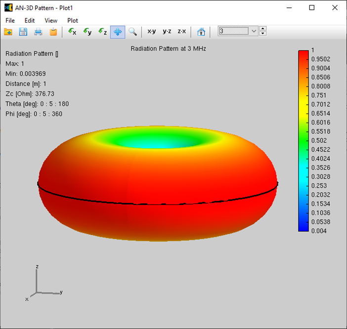
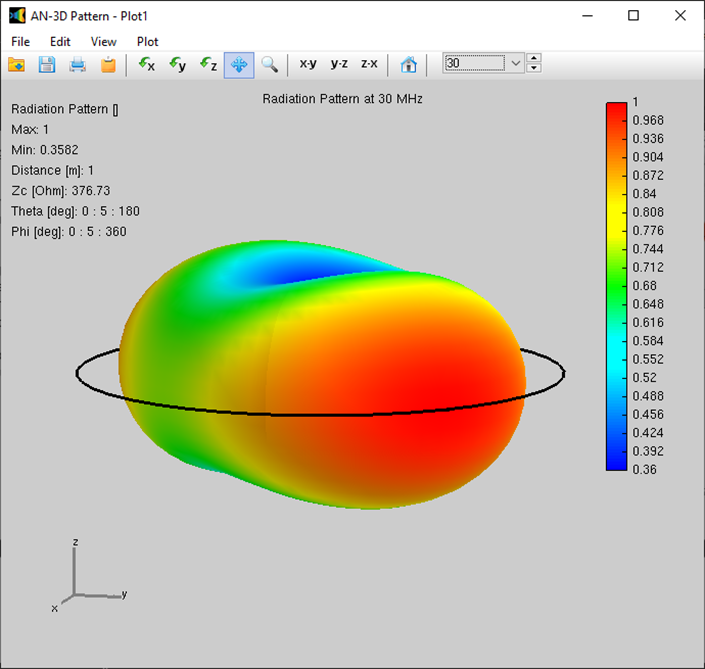
See Also:
Explore the design and simulation of monopole antennas over imperfect ground using AN-SOF. Learn how ground conditions impact performance and optimize efficiency for LF/MF broadcasting applications.
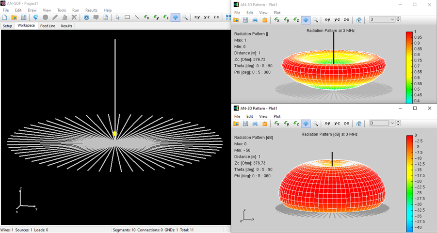
Introduction
A monopole antenna is a class of radio antenna consisting of a single radiating element, typically mounted vertically over a conductive ground plane. It is one of the simplest and most widely used antenna designs, particularly in applications where space and simplicity are critical. The monopole can be thought of as half of a dipole antenna: by introducing a ground plane, one of the dipole’s two radiating elements is effectively replaced by the ground plane’s mirror image, creating a virtual “second leg.” This results in a structure that is electrically equivalent to a dipole but requires only half the physical height, making monopoles particularly advantageous for low-frequency and compact installations.
Monopole antennas are commonly used in a variety of applications, including AM/FM broadcasting, LF (Low Frequency) and MF (Medium Frequency) communication systems, mobile and base station antennas, and amateur radio setups. Their omnidirectional radiation pattern in the horizontal plane makes them ideal for broadcasting and communication over wide areas. However, their performance is highly dependent on the quality of the ground plane, as losses in the ground can significantly reduce efficiency and gain.In this article, we will simulate a monopole antenna in the form of a radio mast operating over imperfect ground, typical of LF and MF broadcasting scenarios. We will explore the impact of ground conditions on antenna performance and demonstrate how to optimize the design for improved efficiency.
Step 1 | Setup
Navigate to the Setup tab and set the operating frequency to 3 MHz in the Frequency panel. Next, go to the Environment panel > Ground Plane box and select the Real option, as shown in Fig. 1. Choose the Radial wire ground screen and Poor ground options. Note that the soil conductivity will automatically be set to 0.001 S/m and the relative permittivity (dielectric constant) to 5.
Finally, configure the number of radials, their length, and their radius as illustrated in Fig. 1. For radio masts, it is common practice to use a constant input power as a reference, such as 1 kW. Proceed to the Excitation panel, select Discrete Sources, then choose Set Input Power and enter 1,000 W, as shown in Fig. 2.
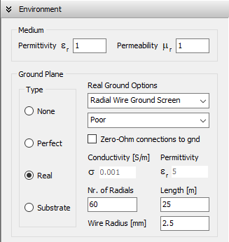
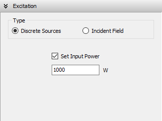
Step 2 | Draw
Right-click on the workspace and select Line from the pop-up menu. Specify a vertical wire with a height of 25 meters (equivalent to 1/4 wavelength at 3 MHz) and a triangular cross-section, as illustrated in Fig. 3. Although the recommended minimum number of segments is 3, we will divide the wire into 10 segments to achieve higher resolution in the current distribution. Note that the wire will automatically be connected to the ground at the origin (0, 0, 0).
Next, right-click on the wire and select the Source/Load command from the pop-up menu. Place a voltage source on the first segment to ensure the source is connected to the base of the mast. For further details, refer to the Adding Sources section.
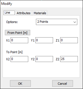
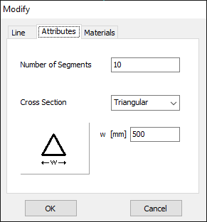
Step 3 | Run
Click on the Run Currents and Far-Field (F11) button located on the toolbar. Once the calculations are complete, click on the Far-Field 3D Plot button on the toolbar to display the radiation pattern. In the AN-3D Pattern window, select Radiation Pattern from the Plot menu to generate the normalized radiation pattern (dimensionless). Then, choose the Radiation Pattern [dB] option to view the pattern in decibel scale. Note that the far field exhibits a null on the xy-plane due to losses in the ground plane, as shown in Fig. 4.
The antenna efficiency is defined as the ratio of radiated power to input power. Navigate to the Metrics tab to view key parameters such as input impedance, VSWR, directivity, gain, and efficiency, as illustrated in Fig. 5. You will observe that the efficiency is relatively low, which consequently results in low gain, as a significant portion of the input power is dissipated in the ground. In this example, we have intentionally chosen a Poor soil condition. To improve antenna efficiency, experiment with different soil types, increase the number of radial wires, and adjust their lengths.
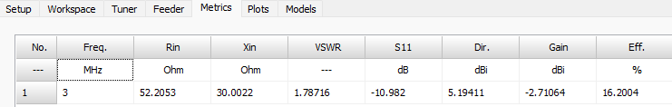
Conclusion
Simulating monopole antennas using the AN-SOF Antenna Simulator offers significant advantages for engineers and designers. By leveraging its advanced modeling capabilities, users can accurately predict antenna performance, optimize designs, and evaluate the impact of various ground conditions without the need for costly and time-consuming physical prototypes.
The ability to analyze parameters such as radiation patterns, input impedance, gain, and efficiency provides invaluable insights, enabling the development of high-performance monopole antennas tailored to specific applications.
Whether you’re designing for LF/MF broadcasting, mobile communications, or amateur radio, AN-SOF empowers you to explore design trade-offs and achieve optimal results with precision and efficiency.
See Also:
Technical Keywords: Monopole Antenna, Imperfect Ground, LF/MF Broadcasting, Radial Wire Ground Screen, Ground Conductivity, Relative Permittivity, Antenna Efficiency, Input Impedance, VSWR, Directivity, Gain, Radiation Pattern, Quarter-wave Monopole, Far-field Analysis, Soil Conditions, Computational Electromagnetics.
Perfect for Beginners: Quick Guide to Helix Antenna Simulation.
Master axial-mode helix design in AN-SOF with this easy step-by-step tutorial. Learn ground plane setup, helix creation, and radiation pattern analysis. Start modeling professional antennas today!
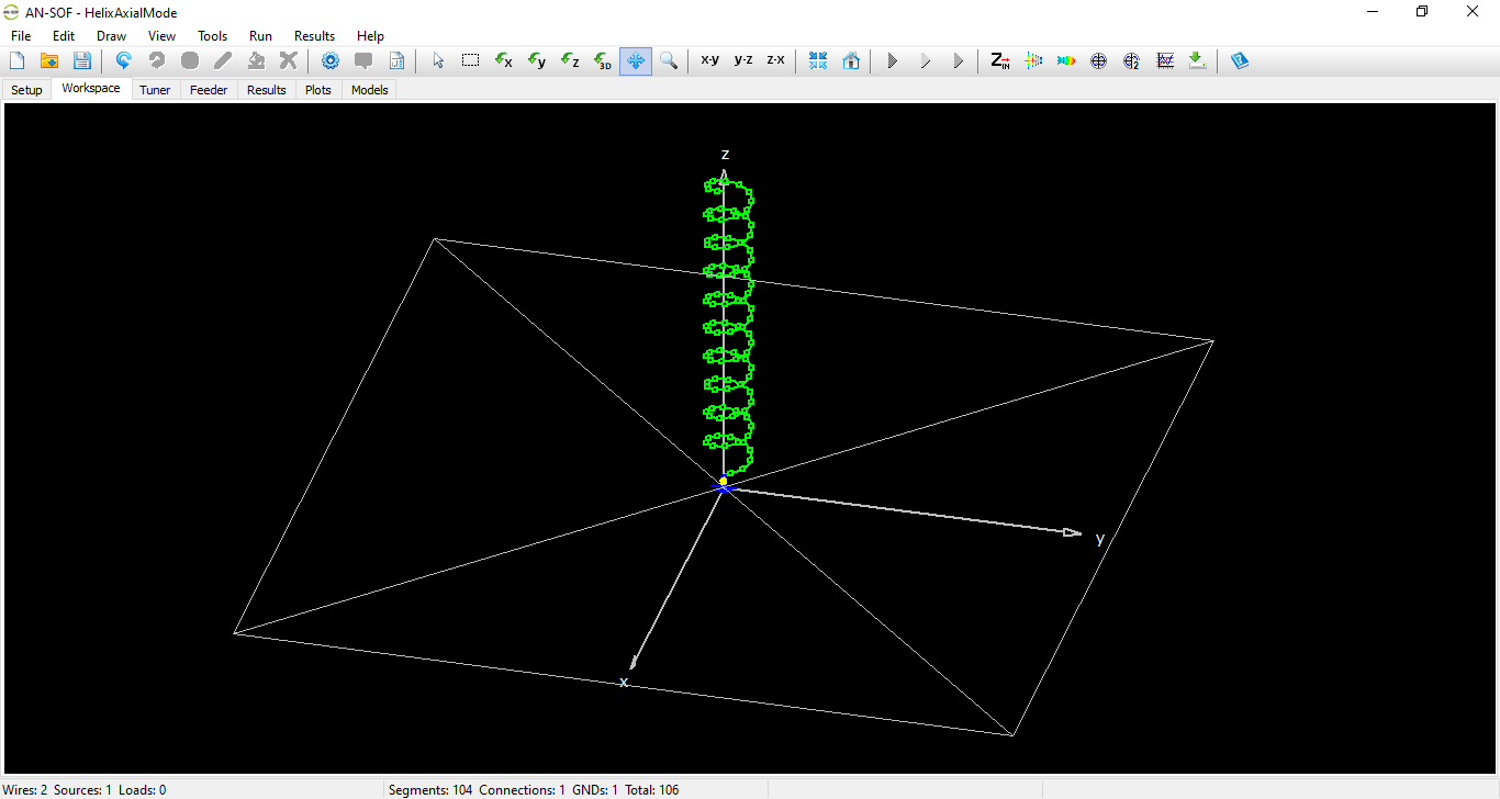
Helix Antenna in Axial Mode
The helix antenna demonstrates the importance of curved segments for accurate geometry representation. When the helix length approaches or exceeds the operating wavelength, it operates in axial mode – characterized by endfire radiation along its axis. This requires a ground plane reflector for proper operation.
Step 1: Setup
- Frequency Setup:
- Navigate to Setup tab > Frequency panel
- Set operating frequency: 100 MHz
- Ground Plane Configuration:
- Go to Environment panel > Ground Plane box
- Select: Perfect
- Set position: Z = 0 (xy-plane) (Fig. 1)
- Excitation:
- Ensure Discrete Sources is selected in Excitation panel
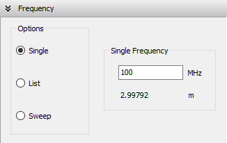
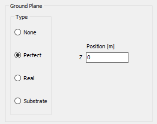
Step 2: Drawing the Structure
- Helix Creation:
- Right-click on the workspace > Select Helix from pop-up menu
- Draw Helix dialog appears (Fig. 2)
- Start point: (0, 0, 0.3) m (above ground plane)
- Orientation: Z-axis
- Axial Mode Dimensions:
- Set parameters per antenna textbooks:
- Radius
- Pitch (turn spacing)
- Number of turns (shown in Fig. 2)
- Attributes tab:
- Segments: 103 (recommended)
- Cross-section: Circular, radius = 3 mm
- Set parameters per antenna textbooks:
- Ground Connection:
- Right-click helix > Start Point to GND
- Draw Line dialog auto-populates connection points (Fig. 3)
- Set:
- Segments: 2
- Radius: 3 mm
- Source Placement:
- Right-click vertical wire > Source/Load/TL
- Connect voltage source to segment nearest ground plane
(Refer to: Adding Sources guide)
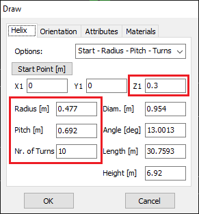
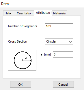
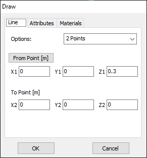
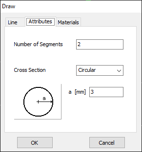
Step 3: Simulation & Analysis
- Run Simulation:
- Click Run Currents and Far-Field (F10)
- View 3D radiation pattern via Far-Field 3D Plot button (Fig. 4a)
- Observe main lobe along helix axis (axial mode characteristic)
- Polarization Analysis:
- In AN-3D Pattern Plot:
- Compare E-right vs. E-left components (Figs. 4b, 4c)
- For accurate comparison:
- Set matching scale maxima (Edit > Preferences)
- In AN-3D Pattern Plot:
- Left-Handed Variant:
- Create by specifying negative turn count
- Re-run simulation and compare polarization components
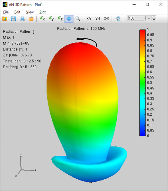
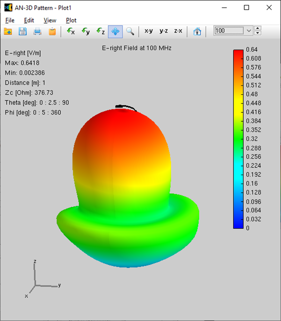
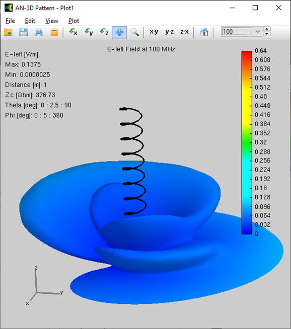
Key Features Demonstrated
- Curved segment modeling for helical structures
- Axial mode radiation characteristics
- Circular polarization analysis
- Ground plane integration
- Parametric comparison (right vs. left-handed)
The complete simulation showcases AN-SOF’s capability to model complex antenna behavior with precise geometrical control.
See Also:
Master Yagi-Uda simulation in AN-SOF! This quick guide walks you through modeling a 3-element array (reflector, driven element, director). Analyze radiation patterns with professional results.
Introduction to Yagi-Uda Antennas
The Yagi-Uda antenna, commonly called simply “Yagi,” is a directional antenna array developed in 1926 by Japanese researchers Hidetsugu Yagi and Shintaro Uda. This elegant design consists of three key elements:
- A driven element (typically dipole)
- Reflectors (usually 1-2 elements)
- Directors (multiple elements)
Through careful spacing of these elements, Yagis achieve high directivity and gain in one direction while being relatively simple to construct. They revolutionized radio communication and remain popular today for applications ranging from TV reception to amateur radio.
Yagi-Uda Simulation Basics
Now that you’ve mastered cylindrical antenna basics, let’s progress to antenna arrays. This guide walks you through simulating a classic 3-element Yagi-Uda design (Fig. 1) featuring:
- Director (front element)
- Reflector (rear element)
- Driven element (center dipole)
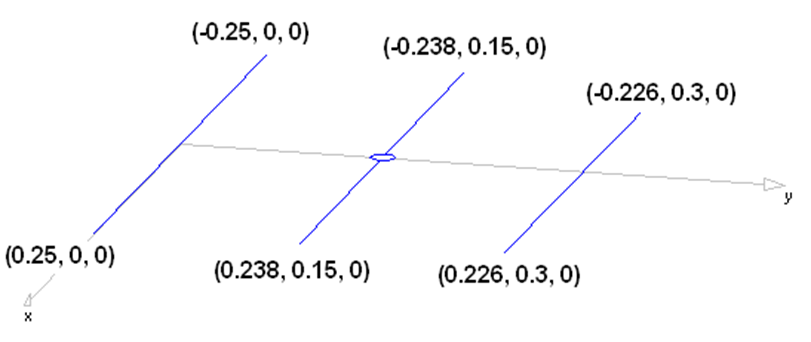
Step 1: Simulation Setup
- Frequency Configuration:
- Setup tabsheet > Frequency panel
- Set: 300 MHz (UHF range ideal for Yagis)
- Environment Settings:
- Environment panel > Ground Plane: Select None (standalone array)
- Excitation panel: Confirm Discrete Sources is active
Step 2: Building the Array
- Element Construction:
- Draw each wire individually (as in cylindrical antenna tutorial)
- Use coordinates from Fig. 1 for precise spacing
- Segment Configuration:
- Uniformly set for all elements:
- Segments: 15 (balanced accuracy/speed)
- Radius: 5 mm (typical for UHF)
- Uniformly set for all elements:
- Source Attachment:
- Right-click driven element > Source/Load/TL
- Connect voltage source to center segment
(Pro Tip: Middle placement ensures symmetrical excitation)
Step 3: Running & Analyzing
- Execute Simulation:
- Click Run Currents and Far-Field (F10)
- Observe 8.7 dBi peak gain in Metrics tab (Fig. 2)
- Radiation Pattern:
- Click Far-Field 3D Plot to visualize:
- Forward-directive beam (Fig. 3)
- Characteristic side/null patterns
- Click Far-Field 3D Plot to visualize:
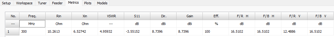
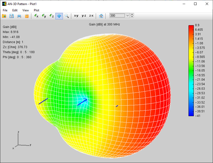
Why This Matters
- Teaches fundamental array principles
- Demonstrates directional gain enhancement
- Provides baseline for more complex designs
(Try modifying element spacing/numbers to see performance changes!)
See Also:
Background Theory
The AN-SOF calculation engine is a high-performance electromagnetic solver written in C++ using double-precision arithmetic. It has been specifically developed to overcome the limitations of traditional wire-antenna modeling and to provide superior accuracy for complex metallic structures.
Conformal Method of Moments (CMoM)
At its core, the engine solves the Electric Field Integral Equation (EFIE) in the frequency domain. While standard solvers utilize the traditional Method of Moments (MoM) with straight-wire approximations, AN-SOF employs the Conformal Method of Moments (CMoM).
In this approach, curved wires are modeled using conformal segments that exactly follow the physical contour of the structure. Traditional linear approximations are often inefficient, requiring a high number of unknowns and excessive computer memory to represent a curve. By using curved segments, AN-SOF significantly reduces the number of unknown currents, simulation time, and memory overhead, allowing for the analysis of much larger and more complex problems.
Overcoming Legacy MoM Limitations
Many legacy MoM codes, especially those based on the thin-wire kernel and linear geometry approximations, suffer from several critical drawbacks that AN-SOF is designed to eliminate:
- Impedance Divergence: Traditional codes often produce divergent input impedances as segment density increases.
- Poor Convergence for Curved Structures: Helices, loops, and spirals are often poorly represented by straight-wire segments, leading to inaccurate results.
- Proximity Singularities: Numerical errors frequently occur when two parallel wires are in close proximity or when a wire is near a lossy ground plane.
Exact Kernel Formulation
By combining CMoM with an exact kernel formulation, AN-SOF removes the reliance on the “thin-wire approximation.” This provides several distinct advantages for the user:
- Enhanced Accuracy: The precision of current distribution and far-field calculations is significantly increased.
- Resource Efficiency: Lower memory usage and faster computation times facilitate the modeling of larger designs on standard hardware.
- Broad Frequency Range: The engine maintains stability across an extreme spectrum, from very low frequencies (60 Hz power circuits) to high-frequency microwave applications.
The foundation of modern antenna simulation lies in solving the Electric Field Integral Equation (EFIE). For metallic structures with ideal conductivity, the EFIE relates the incident electromagnetic wave to the currents induced on the surface of the object.
The Fundamental Equation
In the frequency domain, the EFIE is expressed as follows:
$\displaystyle \hat{\mathbf{n}} \times \left[ j \omega \mu_0 \int_S \mathbf{J}_s(\mathbf{r}’) \, G(\mathbf{r}, \mathbf{r}’) \, d^2\mathbf{r}’ + \frac{j}{\omega \varepsilon_0} \nabla \int_S \nabla’ \cdot \mathbf{J}_s(\mathbf{r}’) \, G(\mathbf{r}, \mathbf{r}’) \, d^2\mathbf{r}’ \right] = \hat{\mathbf{n}} \times \mathbf{E}^{\text{inc}}(\mathbf{r}) \quad (1)$
Where:
- $\mathbf{E}^{\text{inc}}$: The incident electric field on the PEC (Perfect Electrical Conductor) surface $S$.
- $\hat{\mathbf{n}}$: The unit vector normal to the surface at the observation point $\mathbf{r}$.
- $\mathbf{J}_s(\mathbf{r}’)$: The unknown surface electric current density at the source point $\mathbf{r}’$.
- $G$: The free-space Green’s function.
The free-space Green’s function is given by:
$\displaystyle G(\mathbf{r}, \mathbf{r}’) \,=\, \frac{e^{-j k R}}{4 \pi R} \qquad (2)$
where $R = |\mathbf{r} \,-\, \mathbf{r}’|$ is the distance between the source and observation points.
As usual, $k = \omega/c$ is the wavenumber, $\omega = 2\pi f$ is the angular frequency, $f$ is the frequency in Hertz (Hz), and $c = 1/\sqrt{\mu_0 \varepsilon_0}$ is the speed of light in free space. The permeability and permittivity of free space are denoted by $\mu_0$ and $\varepsilon_0$, respectively. The free-space wavelength is defined as $\lambda = c/f$.
The EFIE expresses the boundary condition on a surface $S$, which is assumed to be a Perfect Electrical Conductor (PEC); specifically, it enforces a zero tangential electric field on that surface.
From Surfaces to Wires
When modeling wire antennas, we assume the wire radius ($a$) is much smaller than the wavelength ($a \ll \lambda$). This allows us to simplify the surface integral into a line integral along the axis of the wire. The resulting equation for a curvilinear wire $C$ is:
$\displaystyle \hat{\mathbf{s}} \cdot \frac{j}{\omega\varepsilon_0} \int_C \left[ k^2 I(s’) K(s,s’) \,\hat{\mathbf{s}}’ \,+\, \frac{d I(s’)}{ds’} \nabla K(s,s’) \right] ds’ \,=\, \hat{\mathbf{s}} \cdot \mathbf{E}^{\text{inc}} \qquad (3)$
where $\hat{\mathbf{s}}$ is the tangential unit vector along the curve $C$. In this specialized form, $I(s’)$ represents the total current flowing along the wire’s path $C$, and $K(s, s’)$ is the Kernel of the integral equation, which is given by:
$\displaystyle K(s,s’) \,=\, \frac{1}{4 \pi^2} \int_0^{2\pi} \int_0^{2\pi} G(\mathbf{r},\mathbf{r}’) \, d\phi’ d\phi \qquad (4)$
where $\phi$ and $\phi’$ represent the angular positions of the observation and source points, respectively, on the wire’s circular cross-section.
By averaging the EFIE over the wire circumference, we obtain the curvilinear EFIE presented in Eq. (3), utilizing the exact kernel defined in Eq. (4).
The current distribution $I(s)$ represents the average value of the surface current density $\mathbf{J}_s$ in the axial direction, while current in the transverse direction is neglected. This remains a valid assumption provided the wire radius is small relative to the wavelength $\lambda$.
Parametric Modeling and the Exact Kernel
Accurate simulation of curved wires—such as helices, spirals, or loops—requires a parametric description of the wire’s geometry. By defining the position vector $\mathbf{r}(s)$ and its first derivative (the tangent vector), the solver maintains exact geometric information that is lost in traditional straight-wire approximations.
The wire axis $C$ is described by parametric equations, which can be expressed in a Cartesian coordinate system as:
$\displaystyle \mathbf{r}(s) \,=\, \hat{\mathbf{x}}\ x(s) \,+\, \hat{\mathbf{y}}\ y(s) \,+\, \hat{\mathbf{z}}\ z(s) \qquad (5)$
In this equation, $\mathbf{r}(s)$ points from the origin to any point on the wire, as shown in Fig. 1. The parameter $s$ varies over a real interval $s_{\min} \leq s \leq s_{\max}$.
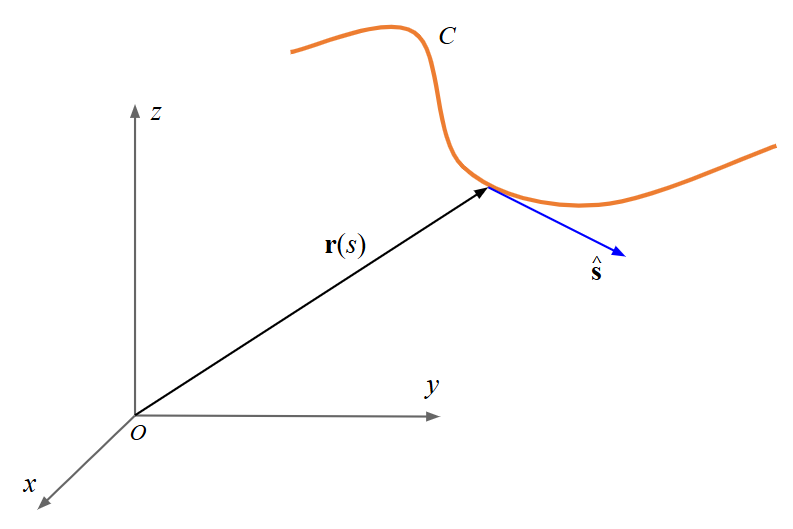
The tangent unit vector $\hat{\mathbf{s}}$ is obtained from the first derivative of Eq. (5):
$\displaystyle \frac{d \mathbf{r}}{ds} \,=\, \hat{\mathbf{x}}\ \frac{dx}{ds} \,+\, \hat{\mathbf{y}}\ \frac{dy}{ds} \,+\, \hat{\mathbf{z}}\ \frac{dz}{ds}\ \implies\ \hat{\mathbf{s}} = \frac{d \mathbf{r}}{ds}\,\Bigg|\frac{d \mathbf{r}}{ds}\Bigg|^{-1} \quad (6)$
This parametric description is essential for the accurate modeling of curvilinear wires and general wire structures. Approximating the geometry with straight-wire segments results in a loss of geometric information that can never be fully restored. However, this information is preserved when a parametric representation is used to describe the wire’s locus.
The Thin-Wire Approximation
In many legacy codes, the exact kernel in Eq. (4) is simplified using the thin-wire approximation (Fig. 2):
$\displaystyle K(s,s’) \approx \frac{e^{-j k R}}{4 \pi R}, \qquad R \,=\, \sqrt{|\mathbf{r}(s) \,-\, \mathbf{r}(s’)|^2 + a^2} \qquad (7)$
where $a$ is the wire radius.

If the wire is straight and $s$ represents the length parameter along the wire, and when the observation point $\mathbf{r}(s)$ and the source point $\mathbf{r}(s’)$ are both on the same straight wire, the distance $R$ reduces to the standard thin-wire approximation for straight wires:
$\displaystyle R \,=\, \sqrt{(s \,-\, s’)^2 + a^2} \qquad (8)$
While this approximation is computationally efficient, it introduces numerical artifacts when segments are very short or when wires are in close proximity. AN-SOF’s use of the Exact Kernel avoids these simplifications, ensuring that the distance $R$ between source and observation points is calculated precisely across the entire tubular surface of the wire. This approach leads to superior convergence and numerical stability.
The kernel is the mathematical core of the Electric Field Integral Equation (EFIE) solved by AN-SOF. It determines how the current at one point on a wire influences the field at another. While several approximations exist to simplify this calculation, AN-SOF utilizes an Exact Kernel to maintain high numerical precision where other solvers fail.
Defining the Kernel
The kernel is obtained by averaging the free-space Green’s function $G(\mathbf{r}, \mathbf{r}’)$ over the circumference of the wire’s cross-section. Mathematically, it is expressed as:
$\displaystyle K(s,s’) \,=\, \frac{1}{4 \pi^2} \int_0^{2\pi} \int_0^{2\pi} G(\mathbf{r},\mathbf{r}’) \, d\phi’ d\phi \qquad (1)$
In this equation:
- $s$ and $s’$ are coordinates along the wire axis (observation and source points).
- $\phi$ and $\phi’$ are the angular positions on the wire’s surface.
- The result represents the interaction between a source point $\mathbf{r} = (s, \phi)$ and an observation point $\mathbf{r}’ = (s’, \phi’)$ on the actual tubular surface of the wire.
The Thin-Wire Approximation
Because the exact integral is difficult to solve analytically, many legacy Method of Moments (MoM) codes use the thin-wire approximation:
$\displaystyle K(s,s’) \approx \frac{e^{-j k R}}{4 \pi R}, \qquad R = \sqrt{|\mathbf{r}(s) \ – \ \mathbf{r}(s’)|^2 + a^2} \qquad (2)$
where $a$ is the wire radius.
This approximation assumes that the current is concentrated on the wire axis and the observation point is on the surface, or vice versa. While efficient for very thin wires, this simplification breaks down as the wire becomes thicker relative to the segment length.
Consequences of Approximation
When a wire is divided into segments where the diameter is larger than the segment length (a ratio $> 1$), the thin-wire approximation introduces significant numerical errors:
- Current Oscillations: The current distribution begins to exhibit non-physical “ripples” or oscillations, particularly near discrete sources (feed points) and at the wire ends.
- Impedance Divergence: As the mesh is refined (more segments added), the input impedance does not settle on a single value. Instead, it diverges, making it impossible to obtain a reliable result.
Figure 1 shows the current distribution in amplitude along a center-fed half-wave dipole obtained using both the thin-wire approximation and the exact kernel. The antenna has been divided into segments with a diameter three times greater than their lengths, resulting in very thick wire segments.
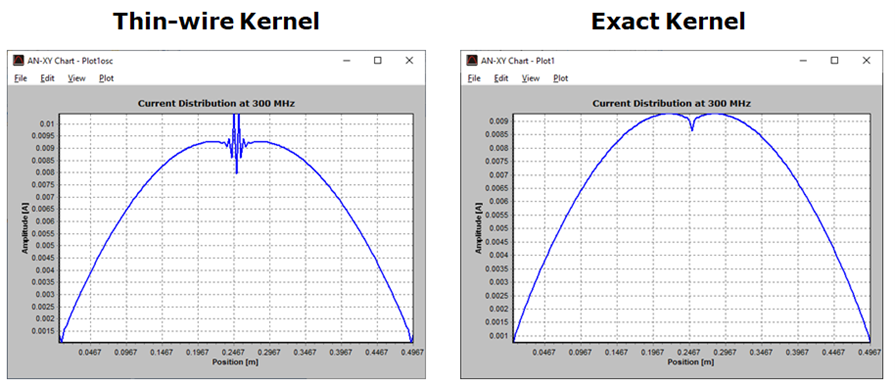
The thin-wire kernel exhibits the well-known oscillatory effect on the current distribution near the position of discrete sources and at wire ends when the segment diameter-to-length ratio is greater than 1. As shown, these oscillations disappear when the exact kernel is used instead of the thin-wire approximation.
The AN-SOF Advantage: Stability and Convergence
By using the Exact Kernel, AN-SOF eliminates these numerical artifacts. The current distribution remains smooth and physically accurate, even for segments with a high diameter-to-length ratio.
As shown in comparisons between AN-SOF and NEC-2 (which relies on the thin-wire kernel), AN-SOF demonstrates monotonic convergence (see Fig. 2). Whether using a finite-gap or delta-gap source, the resistance and reactance values stabilize as the number of segments ($N$) increases, providing a trustworthy solution for complex, high-precision antenna designs.
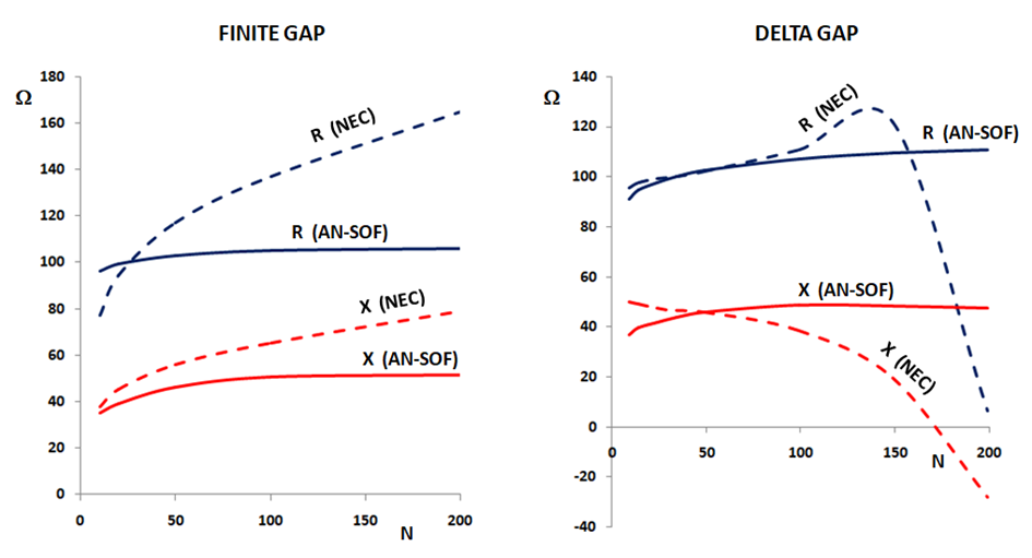
The Method of Moments (MoM) is the numerical technique used by AN-SOF to transform the Electric Field Integral Equation (EFIE) into a system of linear equations. Once digitized, these equations can be solved using standard algebraic methods to determine the current distribution on a structure.
From Calculus to Algebra
To solve the EFIE numerically, we represent the integral linear operator as $\mathcal{L}$. The fundamental equation is expressed as:
$\displaystyle \mathcal{L}(I) \,=\, E_{T} \qquad (1)$
Where $E_{T}$ is the tangential component of the incident electric field on the surface of the wire. Because the exact current distribution ($I$) is unknown, it is approximated as a finite sum of $N$ basis functions ($F_{n}$) with unknown amplitudes ($I_{n}$):
$\displaystyle I \,\approx\, \sum_{n} I_{n} \, F_{n} \qquad (2)$
By substituting this expansion into Eq. (1) and utilizing the linearity of the operator $\mathcal{L}$, we get:
$\displaystyle \sum_{n} I_{n} \, \mathcal{L}(F_{n}) \,=\, E_{T} \qquad (3)$
Weighting and Matrix Formation
To solve for the $N$ unknown amplitudes, Eq. (3) is weighted with a set of $N$ linearly independent testing functions ($T_m$), also known as weighting functions, as follows:
$\displaystyle \sum_n I_n \int T_m \, \mathcal{L}(F_n) \, du \,=\, \int T_m \, E_T \, du \qquad (4)$
where the integrals are evaluated over the wire surface, whose generally curvilinear axis is described parametrically by the real variable $u$. The testing process ensures that the number of independent equations equals the number of unknowns, resulting in the matrix equation:
$[\mathbf{Z}] [\mathbf{I}] \,=\, [\mathbf{V}] \qquad (5)$
Where:
- $[\mathbf{Z}]$ (Impedance Matrix): An $N \times N$ matrix where each element $Z_{mn} = \int T_{m} \, \mathcal{L}(F_{n}) \, du$.
- $[\mathbf{I}]$ (Current Matrix): An $N \times 1$ column vector containing the unknown current amplitudes $I_{n}$.
- $[\mathbf{V}]$ (Voltage Matrix): An $N \times 1$ column vector where each element $V_{m} = \int T_{m} \, E_{T} \, du$.
AN-SOF employs advanced linear algebra algorithms to solve this fully occupied system of equations.
Basis and Testing Functions in AN-SOF
The MoM process begins by dividing the wire structure into $N$ segments. AN-SOF specifically utilizes triangular basis functions and pulse testing functions (Fig. 1).
- Triangular Basis Functions: Used to approximate the current distribution smoothly across segments.
- Pulse Testing Functions: Used to satisfy the boundary conditions along the segments.
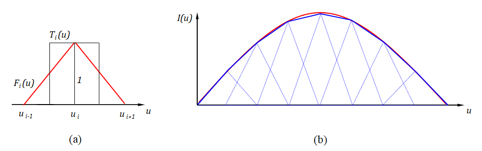
The Conformal Method of Moments (CMoM)
When a wire is curved and described parametrically, the support for the basis and testing functions follows that curve. This results in the Conformal Method of Moments (CMoM). Unlike legacy codes that force basis functions onto straight-wire approximations, CMoM ensures the mathematical model adheres strictly to the physical geometry.
Once the system is solved and the currents ($I_{n}$) are known, the engine can accurately compute secondary parameters such as input impedance, far-field radiation patterns, and near-field distributions.
In the Method of Moments (MoM), the excitation represents the right-hand side of the matrix equation $[\mathbf{Z}] [\mathbf{I}] = [\mathbf{V}]$. This “Voltage Vector” $[\mathbf{V}]$ defines the external electromagnetic energy applied to the structure, which can take the form of discrete voltage sources or incident external fields.
Discrete Voltage Sources
When a voltage generator is placed on a specific wire segment (the $i$-th segment), the corresponding element in the voltage column vector is set to the voltage $V_i$ of that generator. This results in a vector where all elements are zero except for the driven segment:
$\displaystyle [\mathbf{V}] \,=\, \begin{bmatrix} 0 \\ \vdots \\ V_i \\ \vdots \\ 0 \end{bmatrix}$
The Delta-Gap Source Model
In a delta-gap model, the source is assumed to exist at a single point (an infinitesimal gap). In a numerical simulation, this source occupies the entire length of the segment where it is placed. As you increase the number of segments ($N$) to refine the mesh, the length of that segment diminishes, approaching zero. While mathematically convenient, this can lead to convergence issues.
The Finite-Gap Source Model
To model a finite-gap source, which more accurately represents physical connectors, a specific, short wire segment is defined to house the excitation. Unlike the delta-gap model, when the overall antenna mesh is refined, the length of this specific source segment remains fixed. This approach ensures the convergence of the input impedance, which is calculated by dividing the source voltage by the computed current at that specific segment.
Incident Plane Wave Excitation
When the structure is excited by an external source, such as a distant transmitting antenna, it is modeled as an incident plane wave. In this scenario, every segment of the wire is excited simultaneously by the incoming field.
The incident field $\mathbf{E}_i$ at any point $\mathbf{r}$ is defined as:
$\displaystyle \mathbf{E}_i(\mathbf{r}) \,=\, \mathbf{E}_0 \; e^{-j \mathbf{k} \cdot \mathbf{r}}$
Where:
- $\mathbf{k}$: The wavevector, indicating the direction of propagation.
- $k = |\mathbf{k}|$: The wavenumber.
- $\mathbf{r}$: The evaluation point on the structure.
To fill the voltage vector $[\mathbf{V}]$, the solver calculates the contribution for each segment $m$ by integrating the incident field along the segment’s length:
$\displaystyle V_m \,=\, \int_{s_m} \mathbf{E}_i(\mathbf{r}(s)) \cdot \hat{\mathbf{s}} \; ds$
In this integral, $\mathbf{r}(s)$ represents the parametric description of the curved wire axis, and $\hat{\mathbf{s}}$ is the unit vector tangent to the wire at that point. This ensures that only the tangential component of the electric field, the part responsible for inducing current, is accounted for in the calculation (Fig. 1).
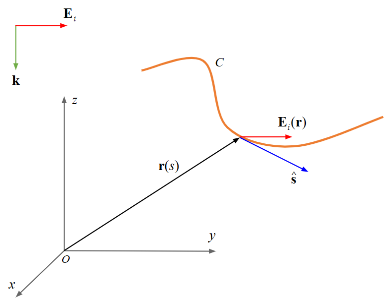
The choice between using curved segments or straight-wire approximations is fundamental to the accuracy and efficiency of electromagnetic simulations. The following study illustrates the advantages of curved segments regarding the stability and convergence properties of numerical solutions.
Helix Antenna Model
To compare these two approaches, we examine a center-fed helical antenna (see Fig. 1) operating in free space (normal mode). The specific dimensions of the model are the following:
- Helix Radius: $0.0273\lambda$
- Pitch: $0.0363\lambda$
- Number of Turns: 10
- Wire Radius: $0.001\lambda$
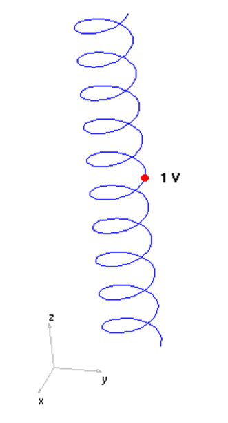
Input Impedance Convergence
The performance of the Conformal Method of Moments (CMoM) in AN-SOF is compared against a standard straight-wire approximation. We investigate the convergence of the input impedance as the number of segments ($N$) increases.
Figure 2(a) shows the Input Resistance convergence. The straight-wire approximation converges much more slowly than the AN-SOF curve, which settles rapidly into a stable value.
Figure 2(b) displays the Input Reactance convergence. The difference is even more pronounced here: the straight-wire model converges very slowly toward a value below the asymptote of the AN-SOF curve. In contrast, the curved segment model in AN-SOF demonstrates smooth, monotonic, and rapid convergence.
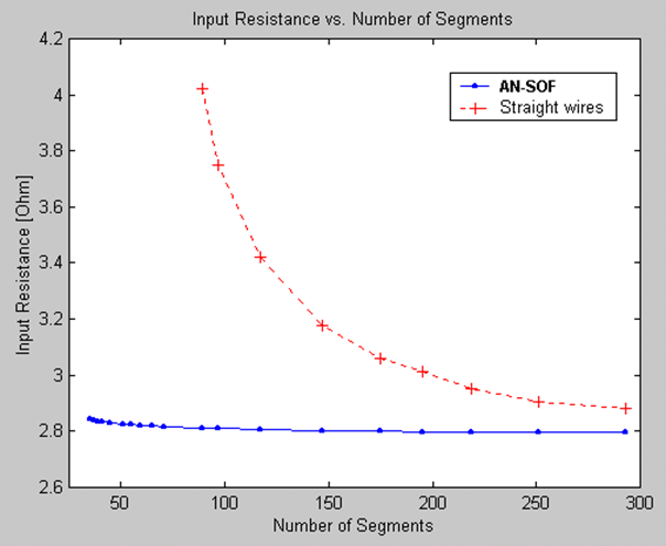
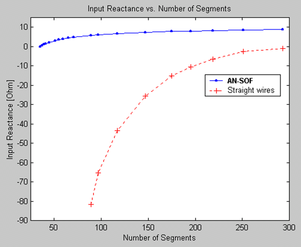
Input Admittance Convergence
The same comparison is applied to the input admittance (conductance and susceptance) to further validate the results.
In Fig. 3(a), the Input Conductance results are plotted. The straight-wire approximation starts to increase smoothly as the number of segments increases and then diverges rapidly. In contrast, the AN-SOF curve decays fast to a convergent value.
In Fig. 3(b), the Input Susceptance is shown. Again, the improved convergence rate of the curved segments is evident, while the straight-wire approximation diverges.
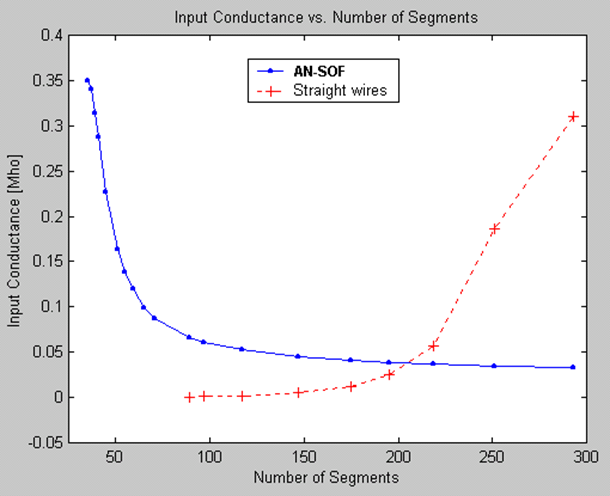
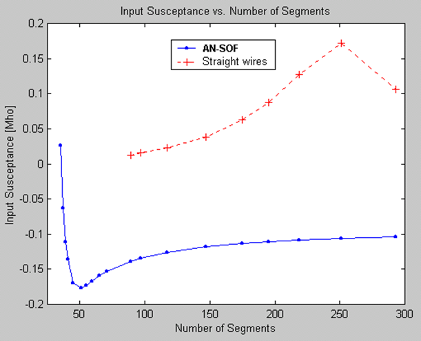
Practical Advantages
As demonstrated by these benchmarks, the use of curved segments provides three critical advantages:
- Convergent Input Impedance and Admittance: As the number of segments is increased, the input impedance and admittance for the CMoM implemented in AN-SOF converge. In contrast, the legacy straight-wire segment approximation does not guarantee convergence, and in the case of the normal-mode helix, it diverges.
- Reduced Simulation Time: Accurate results are obtained with fewer segments, leading to faster computation.
- Memory Efficiency: Because fewer unknowns are required to describe complex geometries like helices, memory overhead is greatly reduced.
By modeling the true physical contour of the structure through the CMoM, AN-SOF ensures that the numerical solution remains stable and reliable, avoiding the artifacts and slow convergence associated with traditional linear approximations.
Frequently Asked Questions
Join a Global Community of RF Experts
Our technical insights are trusted by engineers and antenna enthusiasts at top-tier firms and research institutions. See how they use AN-SOF →